impedance control in pcbs
Impedance Control in PCBs Introduction In the rapidly evolving electronics industry, impedance control in printed circuit boards (PCBs) has become a critical design consideration. As devices become sm...
Introduction
In the rapidly evolving electronics industry, impedance control in printed circuit boards (PCBs) has become a critical design consideration. As devices become smaller and faster, maintaining signal integrity across PCB traces is paramount. Impedance control ensures that signals are transmitted with minimal distortion, which is vital for high-speed and high-frequency applications. Understanding the nuances of PCB layout rules, stackup design, and manufacturing considerations is essential for engineers to deliver reliable and efficient electronic products.
Technical Overview
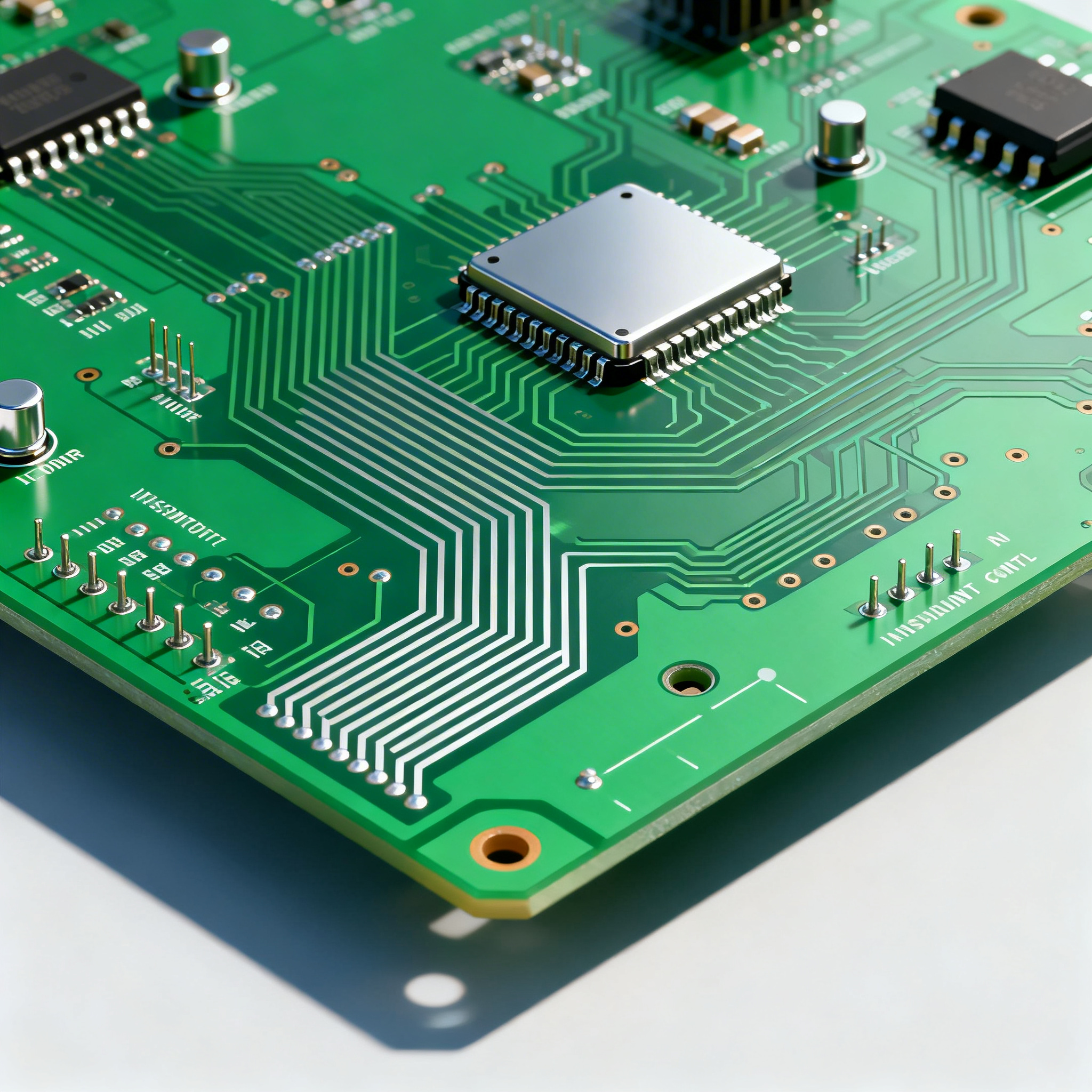
Impedance control in PCBs involves managing the electrical impedance of traces to ensure signal integrity. This is achieved through careful design of trace width, spacing, and the layer stackup. The core principles involve understanding the relationship between signal frequency, trace geometry, and the dielectric properties of the materials used. High-frequency signals are particularly susceptible to impedance mismatches, which can lead to reflection and signal loss. By adhering to established design rules and standards, engineers can mitigate these issues, ensuring optimal performance of the final product.
Detailed Specifications
When designing PCBs with controlled impedance, specific design rules and specifications must be adhered to. These include trace width and spacing, via sizes, and clearances. Such parameters are crucial for maintaining the desired impedance and ensuring signal integrity.
| Parameter | Specification | Importance |
|---|---|---|
| Trace Width | 4 mils - 6 mils | Determines impedance values |
| Trace Spacing | 5 mils - 8 mils | Prevents crosstalk |
| Via Sizes | 0.3 mm - 0.5 mm | Ensures electrical connectivity |
| Clearance | 3 mils - 5 mils | Avoids short circuits |
| Layer Count | 4 layers - 12 layers | Supports complex designs |
| Signal Layer Thickness | 0.5 oz - 1 oz | Affects impedance and current capacity |
| Power/Ground Plane Thickness | 1 oz - 2 oz | Reduces power loss |
| Dielectric Thickness | 0.1 mm - 0.2 mm | Influences impedance |
| Controlled Impedance Tolerance | ±10% | Ensures signal integrity |
| Solder Mask Clearance | 2 mils - 4 mils | Prevents solder bridging |
Key Takeaways from the Specifications
The specifications outlined in the table above are crucial for achieving controlled impedance in PCB designs. Maintaining precise trace widths and spacings is essential to prevent crosstalk and ensure signal integrity. Via sizes and clearances are equally important to uphold electrical connectivity and avoid short circuits. Furthermore, the layer count and thicknesses of signal and power/ground planes play a significant role in supporting complex designs and reducing power loss. These parameters collectively influence the board's performance, making it imperative for designers to adhere to these guidelines.
| Layer Configuration | Description | Applications |
|---|---|---|
| 2-Layer | Simple, low-cost boards | Consumer electronics |
| 4-Layer | Basic multilayer design | Computers, networking devices |
| 6-Layer | Enhanced signal routing | High-speed applications |
| 8-Layer | Complex signal and power management | Telecom, industrial control |
| 10-Layer | Advanced high-frequency designs | Military, aerospace |
| 12-Layer | Highly complex systems | Advanced computing |
| 16-Layer | Maximum design flexibility | Data centers, AI applications |
Practical Implications
The layer stackup options presented highlight the flexibility available to PCB designers in addressing various application requirements. A two-layer board might suffice for simple consumer electronics, whereas a 16-layer configuration offers the complexity needed for high-performance computing applications. The choice of stackup impacts not only the board's electrical performance but also its manufacturing cost and complexity. Understanding these implications helps designers make informed decisions that balance performance with budgetary constraints.
| Material | Dielectric Constant (Dk) | Loss Tangent (Df) |
|---|---|---|
| FR-4 | 4.5 | 0.02 |
| Rogers 4350 | 3.66 | 0.0037 |
| Rogers 4003 | 3.38 | 0.0027 |
| Isola 370HR | 4.04 | 0.019 |
| Nelco N4000-13 | 3.9 | 0.016 |
| Megtron 6 | 3.3 | 0.002 |
| Arlon 85N | 3.5 | 0.004 |
| Polyimide | 4.2 | 0.01 |
| PTFE (Teflon) | 2.1 | 0.001 |
Application Guidelines
The choice of material for a PCB significantly affects its electrical properties and performance. Materials like FR-4 are commonly used due to their cost-effectiveness and adequate performance for many applications. However, for high-frequency designs, materials such as Rogers 4350 or PTFE are preferred due to their lower dielectric constants and loss tangents, which reduce signal loss. Selecting the appropriate material involves considering the application's frequency requirements, budget, and environmental conditions, ensuring optimal performance and reliability.
Design Considerations
Designing PCBs with controlled impedance requires a comprehensive understanding of various factors, including trace geometry, material properties, and signal frequencies. Engineers must consider the dielectric constant of materials, as it influences the impedance of traces. Additionally, the thickness of the dielectric layers and copper traces impacts the overall impedance and must be carefully managed. Simulation tools can assist in predicting the impedance and identifying potential issues before manufacturing. Adhering to IPC standards ensures that the design meets industry requirements for quality and reliability.
Step-by-Step Implementation
Implementing impedance control in PCB design involves several critical steps:
- Define Design Requirements: Begin by identifying the specific impedance requirements for your application, considering factors such as signal frequency and bandwidth.
- Select Appropriate Materials: Choose materials with suitable dielectric properties to meet the impedance and performance criteria.
- Determine Trace Geometry: Calculate the necessary trace width and spacing based on the desired impedance and material properties.
- Design Layer Stackup: Configure the layer stackup to support the impedance goals, considering signal routing and power distribution needs.
- Use Simulation Tools: Employ simulation software to model the impedance and identify potential design issues before manufacturing.
- Adhere to Design Rules: Follow established design rules for trace width, spacing, and via sizes to ensure reliable performance.
- Collaborate with Manufacturers: Work closely with PCB manufacturers to ensure that the design is manufacturable and meets all specifications.
- Perform Prototype Testing: Test prototypes to validate the impedance control and make necessary adjustments before full-scale production.
Common Issues & Solutions
Designing PCBs with controlled impedance can present several challenges. Here are common issues and their solutions:
- Impedance Mismatch: Occurs when the trace impedance does not match the expected value, leading to signal reflection. Use precise calculations and simulations to mitigate this.
- Crosstalk: Caused by inadequate trace spacing, resulting in interference. Ensure sufficient spacing between traces to avoid this issue.
- Signal Loss: High-frequency signals can suffer from excessive loss due to improper material selection. Choose materials with low loss tangents.
- Manufacturing Variability: Variations in manufacturing processes can affect impedance. Collaborate with manufacturers to minimize these discrepancies.
- Environmental Factors: Temperature variations can impact impedance. Design with materials that have stable dielectric properties across temperature ranges.
- Complex Routing: High-density designs can complicate routing. Use multilayer stackups to manage signal paths effectively.
Applications & Use Cases
Impedance-controlled PCBs are critical in various high-speed and high-frequency applications. They are widely used in telecommunications, where signal integrity is paramount for data transmission. In the automotive industry, these PCBs ensure reliable communication between electronic control units. Aerospace and military applications also rely on impedance control to maintain performance in harsh environments. Consumer electronics, such as smartphones and tablets, benefit from controlled impedance to support high-speed data transfer and processing.
Selection & Sourcing Guide
When selecting and sourcing materials and components for impedance-controlled PCBs, consider factors such as material properties, cost, and availability. Reputable suppliers can provide guidance and support in choosing the right materials for your application. For sourcing electronic components, visit IC Online, a comprehensive resource for finding the components you need.
FAQ
- What is PCB impedance control? Impedance control in PCBs involves designing traces with specific impedance values to ensure signal integrity.
- Why is impedance control important? It prevents signal reflection and loss, ensuring reliable performance in high-speed and high-frequency applications.
- How do I calculate trace impedance? Use formulas and simulation tools that consider trace geometry, material properties, and layer stackup.
- What are common materials used for impedance-controlled PCBs? FR-4, Rogers, and PTFE are commonly used materials, each with specific dielectric properties.
- How does layer stackup affect impedance? The configuration of layers influences signal routing and power distribution, affecting overall impedance.
- Can I use standard PCBs for high-speed applications? Standard PCBs may not offer the necessary impedance control, making specialized designs necessary for high-speed applications.
- What role do vias play in impedance control? Vias connect different layers, and their size and placement can impact impedance and signal integrity.
- How can I ensure my design meets impedance specifications? Collaborate with manufacturers and use simulation tools to validate the design before production.
- What challenges might I face in designing impedance-controlled PCBs? Common challenges include impedance mismatch, crosstalk, and signal loss, which can be addressed through careful design and material selection.
- Where can I find reliable PCB manufacturers? Companies like PCBWay and Nova PCBA offer professional PCB manufacturing services.
Conclusion
Impedance control in PCBs is a vital aspect of modern electronic design, ensuring signal integrity and performance in high-speed applications. By understanding the technical specifications, design considerations, and material properties, engineers can create reliable and efficient PCBs. Collaborating with manufacturers and leveraging simulation tools further enhances the design process, leading to successful implementation and production of impedance-controlled PCBs.