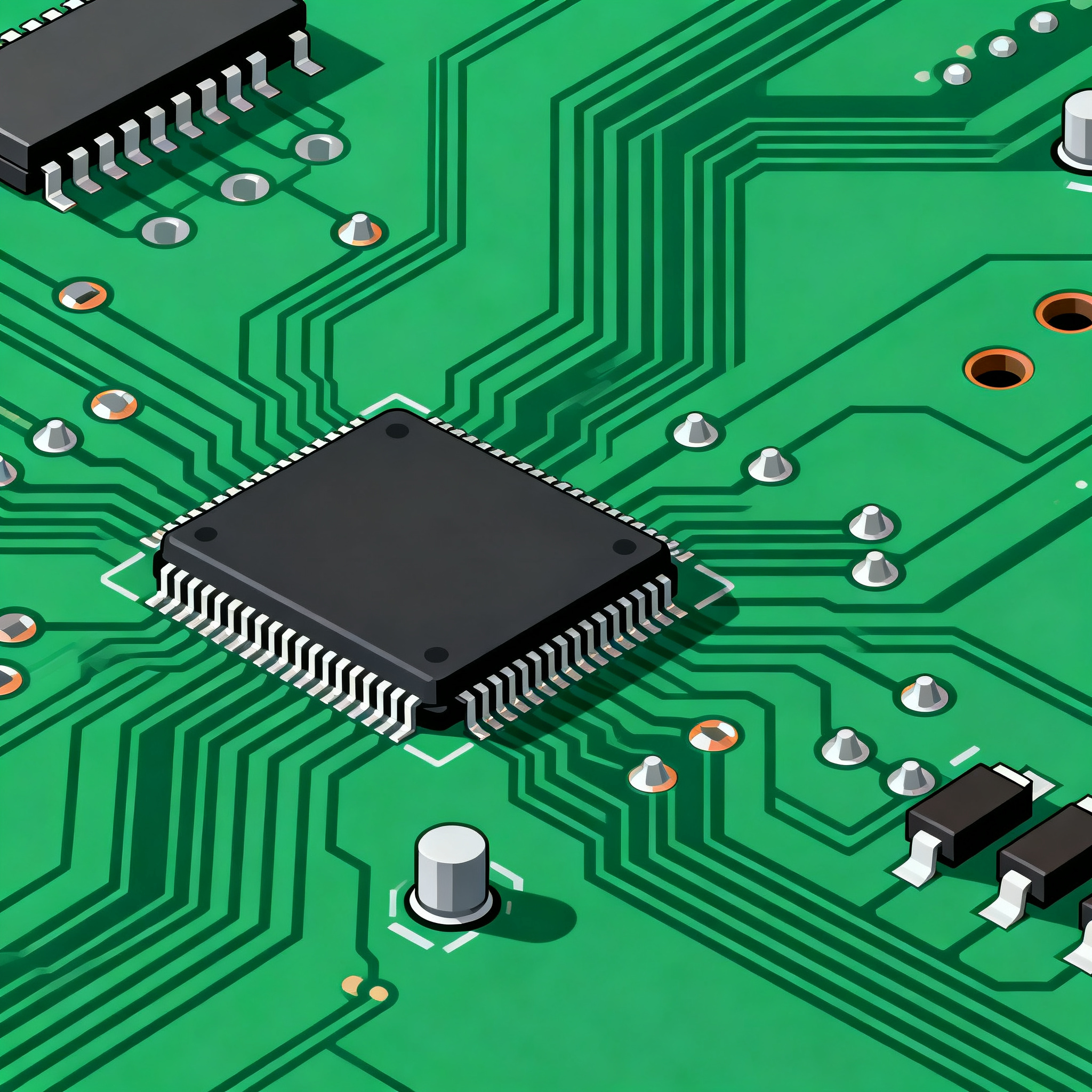
Identifying and Resolving PCB Assembly Defects: A Troubleshooting Guide for 2026
Identifying and Resolving PCB Assembly Defects: A Troubleshooting Guide for 2026 Introduction In the rapidly advancing field of electronics, printed circuit boards (PCBs) form the backbone of virtuall...
Introduction
In the rapidly advancing field of electronics, printed circuit boards (PCBs) form the backbone of virtually every electronic device. As we move towards 2026, the complexity and miniaturization of PCBs continue to increase, making it imperative for engineers to understand and resolve potential assembly defects. This guide aims to provide a comprehensive look at PCB layout rules, stackup design, signal integrity, and manufacturing considerations, all of which are crucial for successful PCB assembly and function.
Technical Overview
Printed Circuit Boards (PCBs) serve as the foundation for electronic circuits, providing mechanical support and electrical connections between components. The core concepts of PCB design include the understanding of trace routing, signal integrity, and layer stackup. These principles ensure that signals are transmitted without interference and that the board can withstand the operational environment. Adhering to industry standards, such as those provided by the IPC, ensures that PCBs meet quality and reliability requirements.
Signal integrity, in particular, is a major consideration in PCB design. It involves ensuring that the electrical signals within the board are transmitted with minimal loss and distortion. This requires careful planning of trace widths, spacing, and via sizes, as well as a thorough understanding of the materials used in PCB construction. The choice of materials, such as FR-4 or Rogers, affects the dielectric constant and loss tangent, which in turn impacts the performance of high-frequency circuits.
Detailed Specifications
Specifications in PCB design are critical as they define the physical and electrical properties of the board. These include trace width, spacing, via sizes, and clearances, which are essential for maintaining signal integrity and ensuring manufacturability. Below is a detailed table that outlines the essential PCB design rules.
| Design Parameter | Specification | Comments |
|---|---|---|
| Minimum Trace Width | 5 mils | Depends on current carrying capacity |
| Minimum Trace Spacing | 6 mils | Prevent short circuits |
| Via Hole Size | 10 mils | Standard for signal vias |
| Pad Clearance | 8 mils | Ensure manufacturability |
| Annular Ring | 4 mils | Minimum for reliable connections |
| Silkscreen Clearance | 4 mils | Avoid covering pads |
| Board Edge Clearance | 10 mils | Prevent damage |
| Power Plane Clearance | 20 mils | Avoid shorting |
| Controlled Impedance Tolerance | ±10% | Critical for high-speed designs |
| Copper Thickness | 1 oz/ft² | Standard for most applications |
| Aspect Ratio | 10:1 | Via depth to diameter ratio |
Key Takeaways from the Specifications
The design specifications outlined in the table are fundamental to ensuring the functionality and reliability of a PCB. Minimum trace width and spacing are critical for preventing short circuits and ensuring that traces can handle the required current. Via sizes and pad clearances impact the board's manufacturability, influencing factors such as solderability and mechanical strength. Understanding these specifications allows engineers to design PCBs that meet both electrical and physical requirements, ensuring high performance and reliability.
Layer Stackup Options
Layer stackup is a crucial aspect of PCB design, particularly for high-speed and high-frequency applications. The stackup configuration affects signal integrity, thermal management, and manufacturing complexity. Below is a table that presents various layer stackup options and their typical applications.
| Stackup Type | Layer Configuration | Applications |
|---|---|---|
| 2-Layer | Signal, Ground | Simple designs, low cost |
| 4-Layer | Signal, Ground, Power, Signal | Medium complexity, better EMI |
| 6-Layer | Signal, Ground, Power, Ground, Signal | Improved signal integrity |
| 8-Layer | Signal, Power, Ground, Signal, Ground, Power, Signal | High-speed digital circuits |
| 10-Layer | Signal, Ground, Power, Signal, Ground, Signal, Power, Ground, Signal | Advanced RF designs |
| 12-Layer | Multiple Signal and Power Planes | Complex systems, high density |
| 14-Layer | Custom configurations | Specialized applications |
Practical Implications
Choosing the right layer stackup is essential for optimizing the performance and cost of a PCB. A 2-layer stackup is suitable for simple designs with low-cost constraints, while a 4-layer configuration provides better electromagnetic interference (EMI) control. For complex, high-speed designs, an 8-layer or 10-layer stackup offers improved signal integrity and reduced crosstalk. Engineers must consider the specific requirements of their application, including signal speed, power distribution, and thermal management, when selecting a stackup configuration.
Material Properties
The choice of PCB material significantly influences the electrical performance, thermal stability, and cost of the board. Key material properties include dielectric constant and loss tangent, which affect signal transmission and power loss. Below is a table detailing the properties of common PCB materials.
| Material | Dielectric Constant (Dk) | Loss Tangent (Df) |
|---|---|---|
| FR-4 | 4.2 - 4.8 | 0.020 |
| Rogers 4350B | 3.48 | 0.0037 |
| Rogers 4003C | 3.38 | 0.0027 |
| Isola FR408HR | 3.66 | 0.009 |
| Nelco N4000-13 | 3.7 | 0.010 |
| Polyimide | 4.0 - 4.2 | 0.004 |
| PTFE | 2.1 | 0.001 |
| Arlon 85N | 3.5 | 0.004 |
| Megtron 6 | 3.3 | 0.002 |
| Thermoset | 4.7 | 0.020 |
Application Guidelines
Understanding the material properties of PCBs is essential for optimizing performance in specific applications. FR-4 is a versatile and cost-effective choice for general-purpose boards. For high-frequency applications, materials like Rogers 4350B and PTFE offer lower dielectric constants and loss tangents, minimizing signal loss and distortion. The selection of material should align with the operating frequency, thermal requirements, and budget constraints of the project. Proper material selection ensures reliable performance and longevity of the PCB.
Design Considerations
When designing a PCB, engineers must consider a variety of factors to ensure optimal performance and manufacturability. These considerations include:
- Signal Integrity: Ensure minimal signal loss and interference by carefully planning trace routing and stackup configuration.
- Thermal Management: Use thermal vias and heat sinks to dissipate heat effectively, especially in high-power applications.
- Component Placement: Strategic placement of components can reduce trace length and improve signal integrity.
- Power Distribution: Design power planes to provide stable voltage levels and minimize voltage drop.
- EMI/EMC Compliance: Follow best practices for grounding and shielding to minimize electromagnetic interference.
- Manufacturability: Ensure that design rules align with manufacturing capabilities to avoid defects and reduce production costs.
By addressing these considerations, engineers can design PCBs that are not only functional but also cost-effective and reliable.
Step-by-Step Implementation
- Define Requirements: Begin by defining the electrical, mechanical, and environmental requirements of your PCB project.
- Create a Schematic: Design the circuit schematic using CAD software, ensuring all components and connections are accurately represented.
- Design Layout: Convert the schematic into a PCB layout, adhering to design rules for trace width, spacing, and clearances.
- Choose Materials: Select appropriate materials based on application requirements, considering factors like dielectric constant and thermal performance.
- Optimize Stackup: Determine the optimal layer stackup for your design, balancing performance with cost.
- Run Simulations: Use simulation tools to analyze signal integrity and thermal performance, making adjustments as needed.
- Generate Gerber Files: Once the design is finalized, generate Gerber files for manufacturing, ensuring all layers are correctly represented.
- Prototype and Test: Manufacture a prototype of your PCB and perform thorough testing to identify and resolve any defects.
By following these steps, engineers can systematically design and implement PCBs that meet project specifications and performance requirements.
Common Issues & Solutions
PCBs can encounter various issues during design and manufacturing. Here are some common problems and their solutions:
- Signal Crosstalk: Increase spacing between traces or use ground planes to minimize interference.
- Thermal Overheating: Implement thermal vias and heat sinks to dissipate excess heat.
- Insufficient Solder Mask: Ensure proper solder mask coverage to prevent shorts and improve reliability.
- Component Misalignment: Use fiducials and alignment marks to ensure precise component placement.
- Via Failure: Adhere to aspect ratio guidelines to prevent mechanical failure of vias.
- Impedance Mismatch: Use controlled impedance traces for high-speed signals to prevent reflection and signal loss.
By identifying and addressing these issues early in the design phase, engineers can avoid costly rework and ensure reliable PCB performance.
Applications & Use Cases
PCBs are used across a wide range of industries and applications, including:
- Consumer Electronics: Smartphones, tablets, and laptops rely on PCBs for compact and efficient circuit integration.
- Automotive: Advanced driver-assistance systems (ADAS) and infotainment systems use PCBs for processing and connectivity.
- Telecommunications: High-speed data transmission in networking equipment is facilitated by PCBs with controlled impedance.
- Medical Devices: PCBs in medical equipment must meet stringent reliability and safety standards.
- Aerospace: High-reliability PCBs are used in avionics and satellite systems, where performance is critical.
Each application has unique requirements, and selecting the appropriate design and materials is crucial for success.
Selection & Sourcing Guide
When selecting and sourcing components for PCB design, consider the following:
- Choose components from reputable suppliers to ensure quality and reliability.
- Verify component specifications to ensure compatibility with your design requirements.
- Consider lead times and availability to avoid production delays.
- Use online resources like IC Online to compare options and find the best deals.
By carefully selecting and sourcing components, engineers can reduce costs and improve the overall quality of their PCBs.
FAQ
- What is the importance of PCB design rules?
PCB design rules ensure that the board can be manufactured reliably and functions as intended. They help prevent issues such as short circuits and signal interference.
- How does layer stackup affect signal integrity?
Layer stackup affects signal integrity by influencing factors like impedance and crosstalk. Proper stackup design minimizes signal loss and distortion.
- What materials are best for high-frequency applications?
Materials like Rogers 4350B and PTFE are ideal for high-frequency applications due to their low dielectric constant and loss tangent.
- How can I prevent thermal issues in my PCB design?
Use thermal vias, heat sinks, and appropriate materials to dissipate heat effectively and prevent overheating.
- What are common causes of via failure?
Common causes include improper aspect ratios and mechanical stress. Adhering to design guidelines helps prevent failure.
- Why is controlled impedance important?
Controlled impedance is crucial for high-speed signals to prevent reflection and signal loss, ensuring reliable data transmission.
- How can I ensure EMI/EMC compliance?
Follow best practices for grounding and shielding, and consider using ferrite beads and filters to minimize electromagnetic interference.
- What should I consider when selecting PCB materials?
Consider factors like dielectric constant, thermal performance, and cost to select materials that meet your design requirements.
- How do I test a prototype PCB?
Perform electrical tests to verify connectivity and functionality, and use thermal imaging to assess heat distribution.
Conclusion
In conclusion, successful PCB design and assembly require a deep understanding of design rules, material properties, and manufacturing considerations. By following industry standards and best practices, engineers can create reliable and efficient PCBs that meet the demands of modern electronic applications. This guide provides the foundational knowledge needed to identify and resolve common assembly defects, ensuring optimal performance and longevity of PCB designs.