Identifying and Resolving Common PCBA Soldering Defects: A Troubleshooting Guide
Identifying and Resolving Common PCBA Soldering Defects: A Troubleshooting Guide table { border-collapse: collapse; width: 100%; margin: 20px 0; } th, td { border: 1px solid #ddd; padding: 8px; } th {...
Introduction
Printed Circuit Board Assembly (PCBA) is a critical process in electronics manufacturing, where the performance of the final product heavily depends on the precision of the soldering process. Common soldering defects such as solder bridges, cold joints, and tombstoning can significantly affect the functionality and reliability of electronic devices. Understanding and addressing these defects is crucial for ensuring high-quality PCBA, which is why industry standards like those from IPC and resources from PCB manufacturers such as PCBWay and Nova PCBA are invaluable.
Technical Overview
PCBA involves multiple steps, including component placement and soldering, each of which can introduce defects if not properly controlled. The architecture of a PCB, including its layout, layer stackup, and material selection, plays a vital role in minimizing these defects. Effective soldering, which ensures good electrical and mechanical connections, relies on precise temperature control, solder paste quality, and proper PCB design. Signal integrity and manufacturing considerations, such as trace width and spacing, are fundamental to reducing the risk of defects.
Detailed Specifications
In PCB design, adhering to specific design rules is essential to prevent defects and ensure manufacturability. These specifications include trace width, spacing, via sizes, and clearances. Below is a table outlining key PCB design rules that are instrumental in achieving a defect-free PCBA.
| Design Rule | Parameter | Typical Value |
|---|---|---|
| Trace Width | Minimum | 6 mils |
| Trace Spacing | Minimum | 6 mils |
| Via Diameter | Minimum | 12 mils |
| Annular Ring | Minimum | 4 mils |
| Clearance | Component to Edge | 10 mils |
| Pad Diameter | Minimum | 20 mils |
| Solder Mask Clearance | Minimum | 3 mils |
| Drill Hole Size | Minimum | 8 mils |
| Aspect Ratio | Max | 10:1 |
| Silkscreen Clearance | Minimum | 6 mils |
| Power/Ground Plane Clearance | Minimum | 20 mils |
| Route Width | Controlled Impedance | 8 mils |
Key Takeaways from the Specifications
The specifications provided in the table above highlight the critical dimensions and clearances necessary for a robust PCB design. These parameters ensure that the board can be manufactured without issues such as short circuits or signal integrity problems. For instance, maintaining a minimum trace width and spacing prevents accidental shorts and ensures adequate current-carrying capacity. Furthermore, proper via sizes and annular rings are crucial for reliable inter-layer connections.
Layer Stackup Options
Layer stackup is another essential aspect of PCB design that impacts signal integrity and thermal management. Different layer configurations can be used to meet specific design requirements. The table below presents various layer stackup options commonly used in PCB design.
| Stackup Type | Layer Configuration | Applications |
|---|---|---|
| 2-Layer | Signal - Ground | Simple circuits |
| 4-Layer | Signal - Ground - Power - Signal | Complex circuits with EMI considerations |
| 6-Layer | Signal - Ground - Power - Signal - Power - Signal | High-speed designs |
| 8-Layer | Signal - Ground - Power - Signal - Ground - Power - Signal - Ground | High-density designs |
| 10-Layer | Signal - Ground - Power - Signal - Ground - Power - Signal - Ground - Power - Signal | Advanced RF designs |
| 12-Layer | Signal - Ground - Power - Signal - Ground - Power - Signal - Ground - Power - Signal - Ground - Power | Multi-functional systems |
| HDI (High Density Interconnect) | Microvia technology | Smartphones, tablets |
Practical Implications
The layer stackup options outlined above offer flexibility in design and manufacturing, allowing engineers to tailor their PCBs to specific applications. A 4-layer stackup is commonly used in projects requiring good electromagnetic interference (EMI) performance, while a 6-layer stackup is suitable for high-speed designs. HDI technologies, which use microvias, support high-density applications like smartphones and tablets, providing more routing space and better signal performance.
Material Properties
The choice of materials is fundamental to PCB performance, affecting factors such as signal integrity, thermal management, and manufacturability. The following table lists common materials used in PCBs and their properties.
| Material | Dielectric Constant (Dk) | Loss Tangent (Df) |
|---|---|---|
| FR-4 | 4.5 | 0.015 |
| Rogers 4350B | 3.48 | 0.0037 |
| Rogers 4003C | 3.38 | 0.0027 |
| Isola FR408 | 3.75 | 0.009 |
| DuPont Pyralux | 3.4 | 0.0025 |
| Nelco N4000-13 | 3.7 | 0.009 |
| PTFE (Teflon) | 2.1 | 0.001 |
| Arlon 85N | 3.5 | 0.004 |
| Megtron 6 | 3.3 | 0.002 |
| Panasonic R-5575 | 3.6 | 0.006 |
Application Guidelines
The choice of material is critical in determining the electrical performance of a PCB. Materials like FR-4 are widely used for general-purpose applications due to their balance of cost and performance. For high-frequency applications, materials such as Rogers 4350B and PTFE are preferred due to their lower dielectric constant and loss tangent. Selecting the right material involves considering the specific requirements of the application, including frequency range, thermal performance, and cost constraints.
Design Considerations
When designing PCBs, several factors must be considered to ensure manufacturability and performance. Proper trace width and spacing are critical to avoid electrical shorts and ensure adequate current handling. The use of ground and power planes can help reduce EMI and improve signal integrity. Additionally, understanding the thermal properties of materials and incorporating thermal vias can aid in heat dissipation. Designers should also consider the aspect ratio of vias, ensuring they are manufacturable and reliable. Adhering to IPC standards and collaborating with manufacturers like PCBWay and Nova PCBA can help optimize the design for both performance and cost.
Step-by-Step Implementation
- Define Requirements: Start by outlining the specifications and requirements of the PCB, including size, layer count, and material selection.
- Schematic Design: Create a schematic diagram of the circuit, ensuring all components are correctly placed and interconnected.
- PCB Layout: Design the PCB layout, following design rules for trace width, spacing, and via sizes.
- Layer Stackup: Choose an appropriate layer stackup configuration based on signal integrity and EMI considerations.
- Material Selection: Select materials that match the electrical and thermal performance requirements of the design.
- Design Rule Check (DRC): Perform a thorough DRC to catch any potential issues before manufacturing.
- Prototype Fabrication: Work with a reputable manufacturer like Nova PCBA to produce a prototype for testing.
- Testing and Verification: Conduct rigorous testing to verify the functionality and reliability of the PCB, identifying and resolving any defects.
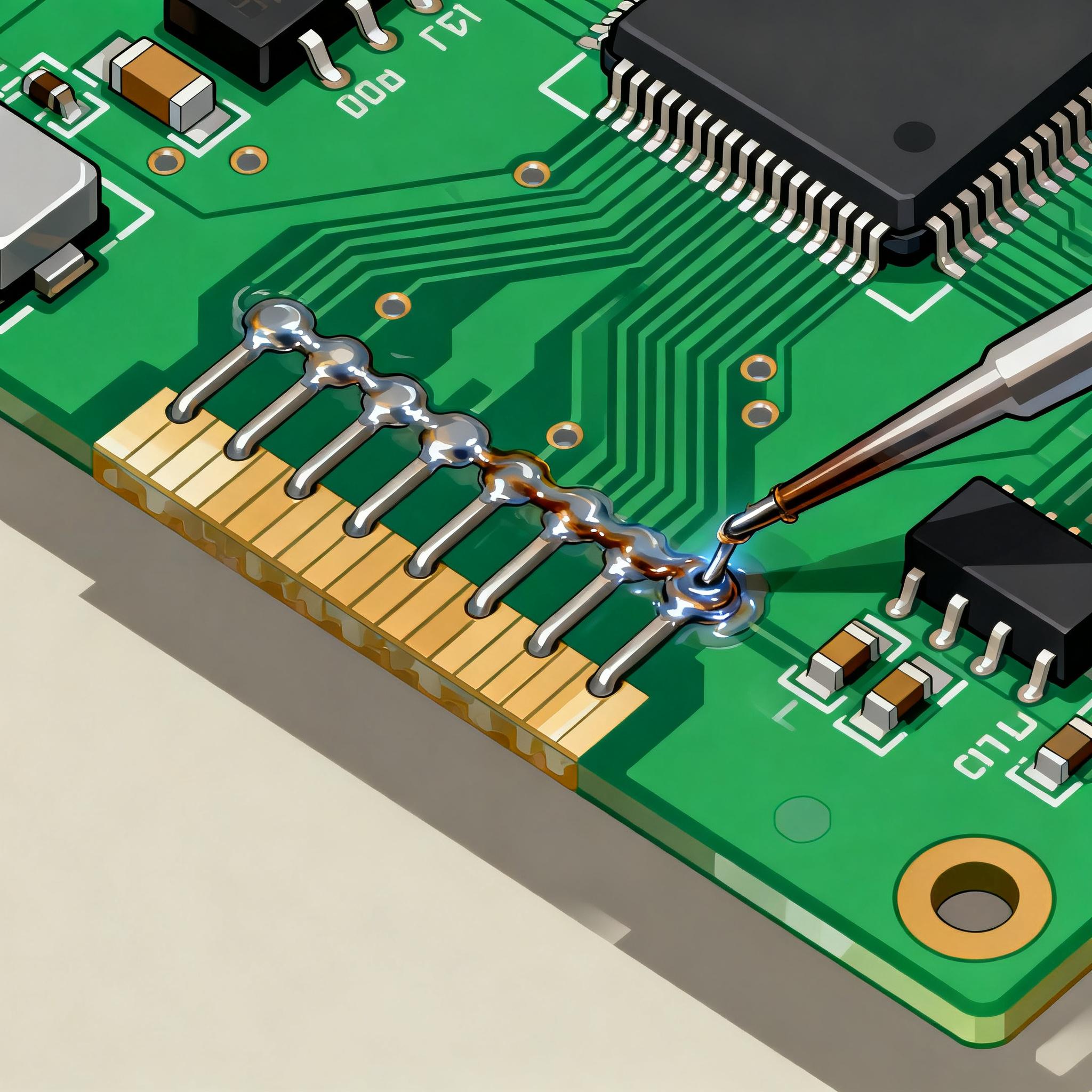
Common Issues & Solutions
- Solder Bridges: Often caused by excessive solder paste or insufficient spacing. Solution: Adjust stencil thickness and ensure proper spacing.
- Cold Joints: Result from inadequate soldering temperature. Solution: Optimize the reflow profile to ensure proper temperature.
- Tombstoning: Occurs when components lift during soldering. Solution: Balance thermal mass and adjust reflow settings.
- Component Misalignment: Caused by inaccurate placement. Solution: Calibrate placement machinery and use fiducials for alignment.
- Open Circuits: Result from missing solder or broken traces. Solution: Ensure complete solder coverage and inspect for trace integrity.
- Delamination: Caused by excessive heat or moisture. Solution: Use materials with better thermal properties and control environmental conditions.
Applications & Use Cases
PCBs are ubiquitous across various industries, powering devices from consumer electronics to automotive and aerospace systems. In consumer electronics, PCBs enable compact and efficient designs in smartphones and wearable devices. In automotive applications, they are used in engine control units and infotainment systems. Aerospace applications demand high-reliability PCBs for navigation and communication systems. Each application requires specific design considerations to meet performance, reliability, and regulatory standards.
Selection & Sourcing Guide
When selecting components and materials for your PCB design, it's essential to consider factors such as availability, cost, and compatibility with your design requirements. Resources like IC Online provide comprehensive databases of electronic components and suppliers, helping designers source the right parts efficiently.
FAQ
- What is the importance of trace width in PCB design? Trace width affects current capacity and signal integrity, making it crucial for reliable PCB performance.
- How do I choose the right layer stackup? Consider factors like EMI, signal integrity, and circuit complexity when selecting a layer stackup.
- What materials are best for high-frequency PCBs? Materials like Rogers and PTFE, which have low dielectric constants and loss tangents, are ideal for high-frequency designs.
- How can I prevent soldering defects? Follow proper design rules, optimize the soldering process, and use quality materials to minimize defects.
- What are common causes of tombstoning? Tombstoning is often caused by uneven heating or solder paste issues; balancing thermal mass can help prevent it.
- Why is a design rule check important? A DRC helps identify potential design errors before manufacturing, saving time and costs.
- What role does signal integrity play in PCB design? Signal integrity ensures that signals are transmitted without distortion, critical for high-speed and high-frequency applications.
- How can thermal management be improved in PCBs? Use thermal vias, heat sinks, and appropriate materials to enhance thermal management.
- What is the significance of IPC standards? IPC standards provide guidelines for reliable and manufacturable PCB designs, ensuring quality and consistency.
- How do I address component misalignment? Ensure accurate placement by calibrating machinery and using fiducials for alignment.
Conclusion
Identifying and resolving common PCBA soldering defects is crucial for producing reliable and high-performing electronic products. By adhering to design rules, selecting suitable materials, and implementing robust manufacturing processes, engineers can minimize defects and enhance product quality. Utilizing resources from IPC, PCBWay, and Nova PCBA, along with thoughtful design considerations, can significantly improve the outcome of PCB projects.