Identifying and Resolving Common PCB Assembly Defects: A Troubleshooting Guide for Engineers
Identifying and Resolving Common PCB Assembly Defects: A Troubleshooting Guide for Engineers Introduction In the rapidly evolving electronics industry, Printed Circuit Boards (PCBs) form the backbone ...
Introduction
In the rapidly evolving electronics industry, Printed Circuit Boards (PCBs) form the backbone of most electronic devices. As devices become more complex and compact, the design and manufacturing of PCBs have become more challenging, making it crucial to identify and resolve common assembly defects. Understanding the intricacies of PCB layout rules, stackup design, and signal integrity is vital for engineers striving to ensure high-quality, reliable products. This article serves as a comprehensive guide for engineers, providing insights into PCB assembly defects and offering practical solutions.
Technical Overview
PCBs are intricate assemblies that require precise design and manufacturing processes. The core concepts of PCB design involve understanding the architecture, layout rules, and principles that ensure signal integrity and operational efficiency. The architecture of a PCB includes various layers, each serving a specific purpose, from signal routing to power distribution. Signal integrity focuses on maintaining the quality of electrical signals as they travel through the PCB, which is influenced by factors like trace width, spacing, and material properties. Manufacturing considerations, such as selecting appropriate materials and adhering to industry standards like IPC, are crucial for minimizing defects and enhancing product reliability.
Detailed Specifications
Specifications are the foundation upon which reliable PCBs are built. They dictate the design rules, material selection, and layer configurations necessary to achieve specific performance criteria. Adhering to these specifications is essential for ensuring signal integrity, minimizing interference, and facilitating efficient manufacturing processes.
| Design Rule | Specification | Importance |
|---|---|---|
| Minimum Trace Width | 5 mil | Ensures current-carrying capability |
| Minimum Trace Spacing | 5 mil | Prevents short circuits |
| Via Diameter | 10 mil | Facilitates layer transitions |
| Annular Ring | 4 mil | Ensures via reliability |
| Clearance to Edge | 10 mil | Prevents physical damage |
| Pad Size | 20 mil | Ensures solderability |
| Drill Hole Size | 8 mil | Accommodates component leads |
| Copper Weight | 1 oz/ft² | Determines current capacity |
| Solder Mask Clearance | 2 mil | Prevents solder bridging |
| Silkscreen Text Height | 40 mil | Ensures readability |
| Aspect Ratio | 8:1 | Ensures manufacturability of vias |
Key Takeaways from the Specifications
The data presented in Table 1 outlines critical design rules that serve as the foundation for reliable PCB manufacturing. Understanding these specifications is crucial for maintaining the integrity of electrical signals and ensuring the durability of the PCB. For instance, adhering to minimum trace width and spacing is essential to prevent overheating and short circuits, while proper via sizes and annular rings are vital for robust electrical connections. These design rules, derived from industry standards like IPC-2221, ensure that engineers can create PCBs that meet both functional and regulatory requirements, ultimately leading to higher quality and more reliable electronic devices.
| Layer Configuration | Number of Layers | Application |
|---|---|---|
| Single Layer | 1 | Simple circuits |
| Double Layer | 2 | Basic consumer electronics |
| Four Layer | 4 | Signal integrity improvement |
| Six Layer | 6 | Advanced routing for complex circuits |
| Eight Layer | 8 | High-speed applications |
| Ten Layer | 10 | Multifunctional devices |
| Twelve Layer | 12 | High-density interconnects |
| Fourteen Layer | 14 | High-performance computing |
Practical Implications
The layer stackup options in Table 2 highlight the versatility and adaptability of PCB designs to meet various application needs. As the number of layers increases, so does the complexity and capability of the PCB. Single and double-layer configurations are suitable for simple and cost-effective designs, while multilayer configurations, such as six and eight layers, offer enhanced signal integrity and are essential for high-speed and high-density applications. Engineers must carefully consider the layer configuration to balance performance requirements with manufacturing costs, ensuring that the chosen stackup aligns with the intended application and budget.
| Material | Dielectric Constant (Dk) | Loss Tangent (Df) |
|---|---|---|
| FR-4 | 4.5 | 0.020 |
| Rogers 4350B | 3.66 | 0.0037 |
| Rogers 4003C | 3.55 | 0.0027 |
| Isola FR408 | 3.75 | 0.0095 |
| Megtron 6 | 3.3 | 0.002 |
| Nelco N4000-13 | 3.7 | 0.008 |
| Arlon 85N | 3.5 | 0.004 |
| Polyimide | 3.5 | 0.0045 |
| Teflon | 2.1 | 0.001 |
Application Guidelines
The material properties outlined in Table 3 play a significant role in determining the performance and suitability of a PCB for specific applications. Dielectric constant and loss tangent are critical parameters that affect signal propagation and loss. Materials like FR-4 are commonly used due to their cost-effectiveness and adequate performance for general applications. However, for high-frequency and high-speed circuits, materials such as Rogers and Megtron 6 offer lower loss tangents, making them ideal for minimizing signal loss and ensuring signal integrity. Engineers must select materials based on the application's frequency requirements, environmental conditions, and cost constraints to optimize performance and reliability.
Design Considerations
When designing a PCB, several practical guidelines must be followed to ensure optimal performance and manufacturability. Firstly, adhering to IPC standards, such as IPC-A-610 for assembly acceptability and IPC-2221 for generic design, is crucial for ensuring quality and consistency. The choice of materials, as highlighted in Table 3, should align with the application's requirements, balancing cost with performance needs. Signal integrity must be a priority, with careful attention to trace routing, impedance control, and minimizing electromagnetic interference (EMI). Design for Manufacturability (DfM) principles should be applied to simplify the assembly process, reduce errors, and lower production costs. Additionally, collaboration with PCB manufacturers early in the design phase can help identify potential issues and optimize the design for the specific fabrication capabilities of the chosen manufacturer.
Step-by-Step Implementation
- Define Requirements: Clearly outline the electrical, mechanical, and environmental requirements for the PCB based on the intended application.
- Select Materials: Choose appropriate materials that meet the dielectric and thermal requirements, considering both performance and cost.
- Design Schematic: Create a detailed schematic that captures all electrical connections and component placements.
- Layout PCB: Follow design rules and guidelines to route traces, place vias, and position components for optimal signal integrity and manufacturability.
- Simulate Design: Use simulation tools to analyze signal integrity, thermal performance, and EMI to identify potential issues.
- Review and Optimize: Conduct design reviews to identify areas for improvement and optimize the layout for performance and manufacturability.
- Prototype and Test: Fabricate a prototype PCB and conduct thorough testing to verify performance against specifications.
- Iterate and Finalize: Make necessary adjustments based on test results and finalize the design for mass production.
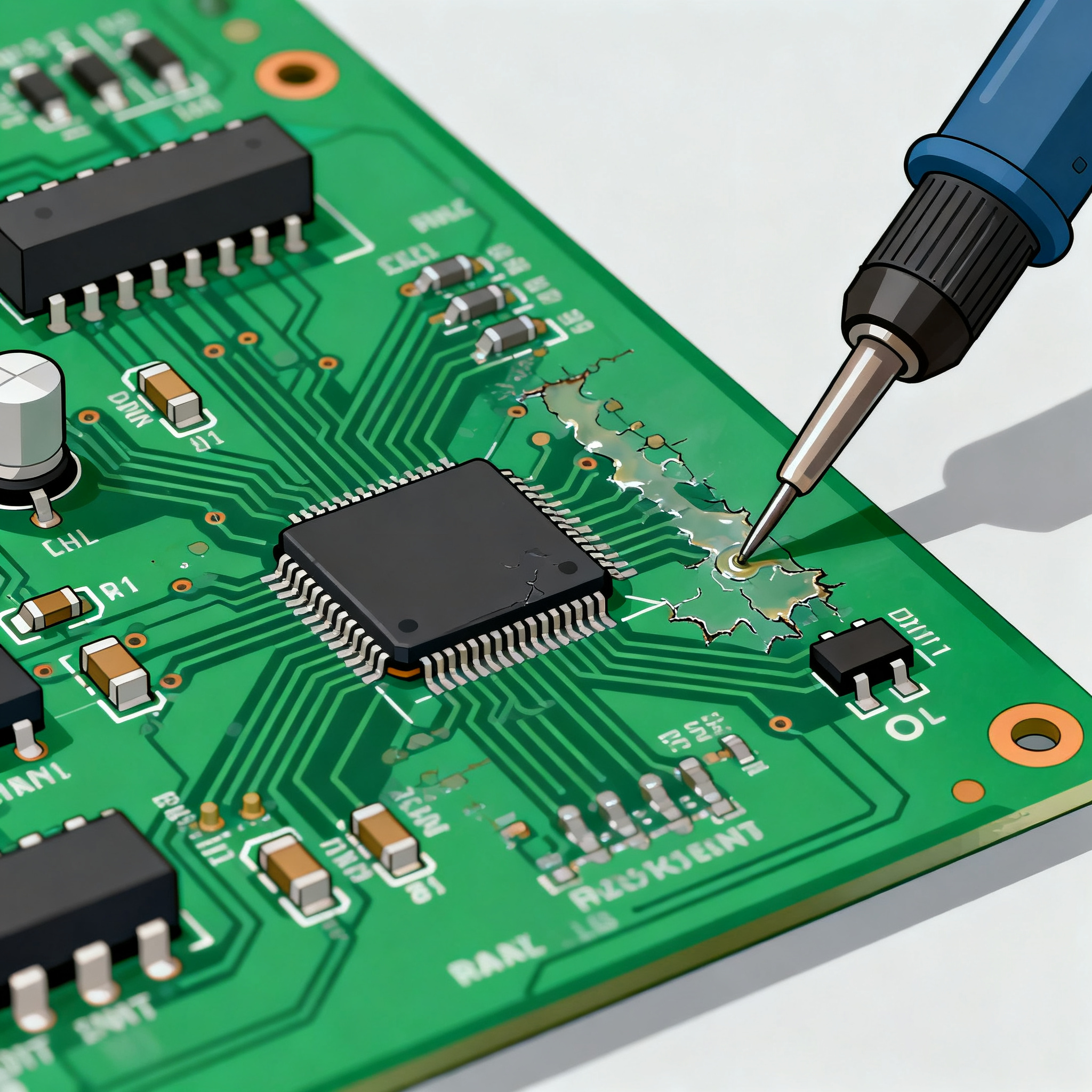
Common Issues & Solutions
- Issue: Solder Bridging — Solution: Ensure proper solder mask application and adjust pad sizes.
- Issue: Component Misalignment — Solution: Use precise pick-and-place machines and verify component footprints.
- Issue: Delamination — Solution: Use materials with high thermal stability and control the lamination process.
- Issue: Electromagnetic Interference (EMI) — Solution: Implement proper grounding and shielding techniques.
- Issue: Insufficient Via Reliability — Solution: Optimize via design and ensure proper plating thickness.
- Issue: Poor Signal Integrity — Solution: Use controlled impedance traces and minimize trace lengths.
Applications & Use Cases
PCBs are integral to a wide range of applications across various industries. In consumer electronics, they form the basis of smartphones, tablets, and home appliances, where compact and cost-effective designs are crucial. In the automotive industry, PCBs are used for control systems, infotainment, and safety features, requiring high reliability and resistance to harsh environments. Advanced applications include aerospace and defense systems, where high-performance PCBs are essential for communication, navigation, and control systems. Each application demands specific design considerations and material selections to meet performance and regulatory standards.
Selection & Sourcing Guide
When selecting and sourcing components for your PCB, consider collaborating with reliable suppliers who offer a wide range of options and competitive pricing. Platforms like IC Online provide access to a vast inventory of electronic components, ensuring that you can find the right parts to meet your design requirements. Evaluate suppliers based on their reputation, lead times, and quality assurance processes to ensure a smooth and efficient procurement process.
FAQ
- What is the minimum trace width for a PCB? The minimum trace width is typically 5 mil, but it can vary based on current requirements and manufacturing capabilities.
- How do I choose the right PCB material? Consider factors like dielectric constant, loss tangent, thermal stability, and cost based on your application's requirements.
- What are common causes of solder bridging? Solder bridging often results from improper solder mask application or oversized pads.
- How can I improve signal integrity? Use controlled impedance traces, minimize trace lengths, and implement proper grounding strategies.
- What is the significance of via reliability? Reliable vias ensure robust electrical connections between layers, critical for the overall functionality of the PCB.
- Why is EMI a concern in PCB design? EMI can disrupt signal transmission and affect the performance of electronic devices, making proper shielding and grounding essential.
- What are design for manufacturability (DfM) principles? DfM principles aim to simplify the manufacturing process, reduce errors, and lower production costs.
- How do I test a PCB prototype? Conduct functional tests, signal integrity analysis, and thermal performance evaluations to verify performance against specifications.
- What factors influence PCB stackup selection? Consider application requirements, signal integrity needs, and cost constraints when choosing a PCB stackup configuration.
- How does layer count affect PCB design? More layers allow for complex routing and improved signal integrity but increase manufacturing complexity and cost.
Conclusion
Identifying and resolving common PCB assembly defects is critical for ensuring the reliability and performance of electronic devices. By adhering to industry standards, selecting appropriate materials, and following best design practices, engineers can minimize defects and enhance product quality. This guide provides valuable insights and practical solutions to help engineers navigate the complexities of PCB design and manufacturing, ultimately leading to successful and reliable electronic products.