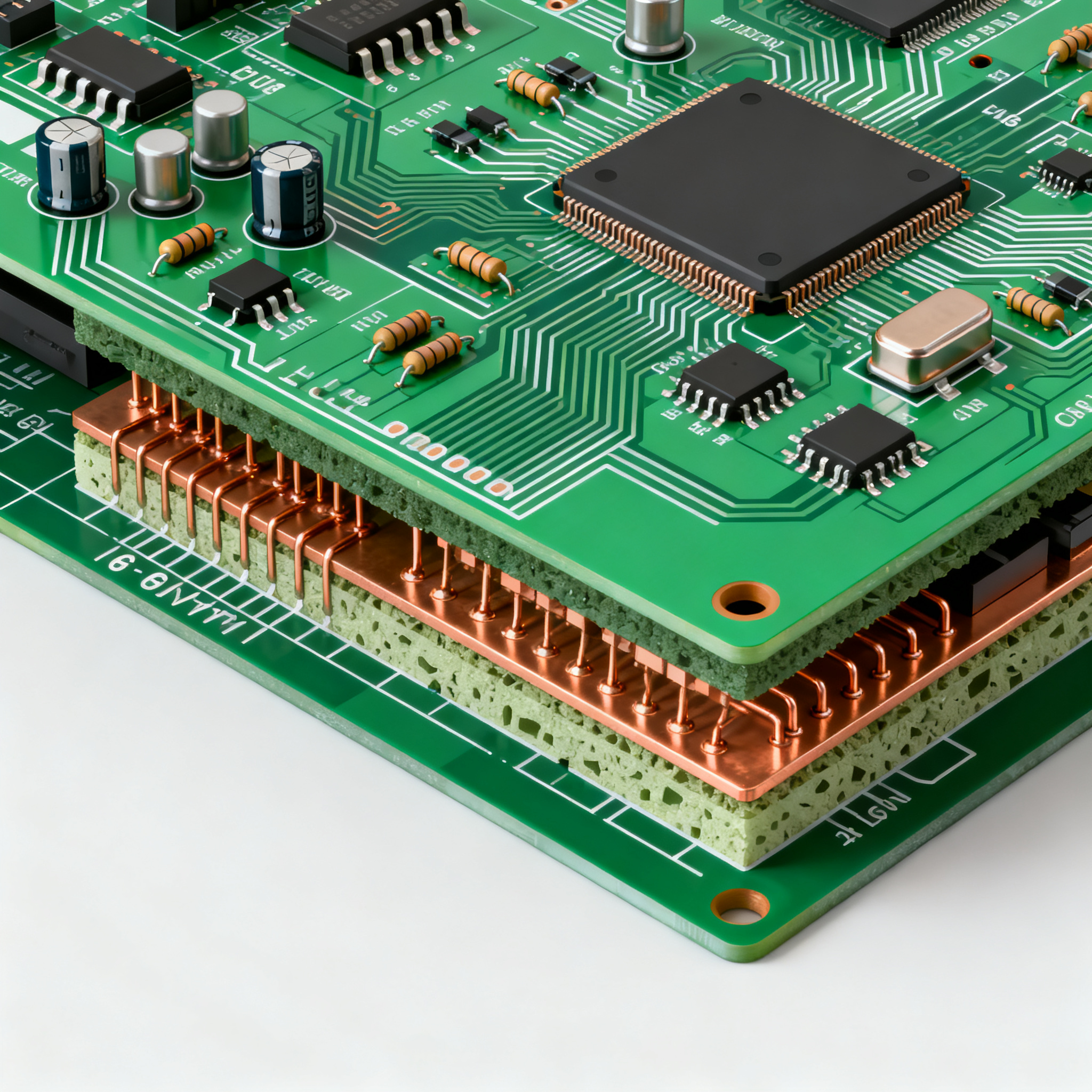
How to Ensure Reliable Consumer Electronics PCB Assembly: Real Examples from 2-Layer to 6-Layer Designs
When Consumer Gadgets Fail: The Hidden Cost of Skipping Traceability and Inspection Last year, a mid-size consumer IoT brand watched its smart plug shipments spike from 50,000 to 200,000 units a month...
When Consumer Gadgets Fail: The Hidden Cost of Skipping Traceability and Inspection
Last year, a mid-size consumer IoT brand watched its smart plug shipments spike from 50,000 to 200,000 units a month—then saw return rates climb past 4% within the first quarter of field deployment. The symptom was intermittent Wi‑Fi disconnects that only appeared after the device had been plugged into a wall outlet for several weeks. Engineering suspected a batch of MLCC capacitors with micro-cracks that opened under thermal cycling, but the contract manufacturer’s records stopped at the date-code level. There was no way to map a specific capacitor reel to the serial numbers of failing boards. Root‑cause analysis dragged on for eight weeks, while the brand absorbed a recall, a retailer chargeback, and a hit to its online ratings.
That scenario isn’t rare; it’s the predictable outcome when assembly traceability is treated as a paperwork exercise instead of a digital thread. End‑to‑end digital tracking requirements now demand that every SMD, BGA, and connector be logged with manufacturer, lot, and date code at receiving, then married to the PCB serial number through the entire SMT line. A manufacturing execution system (MES) that automatically links soldering profiles, AOI results, and functional test data to each board closes the loop. Without it, a latent defect that escapes optical inspection—something that happens more often than many buyers realize—becomes a time bomb.
Automated Optical Inspection (AOI) is often pitched as a safety net, but its effectiveness depends on programming, lighting, and the defect library. One published failure analysis case study showed that misaligned components and lifted leads slipped past AOI when the system wasn’t tuned for the specific package geometry, allowing defects to reach end customers. The same study noted that strict quality checks at every stage, from raw material inspection to final assembly, can push AOI accuracy above 95%. That 5% gap, however, still represents thousands of boards in a high‑volume consumer run—and it’s precisely why traceability must backstop inspection. When a defect does escape, you need to know which 2,000 units share the suspect reel, not which 20,000 units share the suspect month.
Reliability in consumer electronics PCB assembly isn’t just about meeting a spec on paper; it’s about process visibility from reel to serial number. The cost of skipping that visibility is measured in weeks of downtime, brand erosion, and field‑return logistics that far outweigh the incremental investment in digital tracking.
What ‘Reliable’ Really Means in PCB Assembly: Solder Quality, Cleanliness, and Process Control
Ask ten engineers to define “reliable assembly” and you’ll get ten variations, but three pillars consistently separate assemblies that survive years of daily use from those that fail within months: solder joint integrity, contamination control, and automated inspection with closed‑loop feedback. These aren’t abstract ideals; they’re measurable process characteristics that directly prevent field returns.
Solder joint integrity is the most visible indicator. A cold joint, a head‑in‑pillow BGA defect, or insufficient hole fill on a through‑hole connector can pass initial power‑on tests yet crack after a few hundred thermal cycles. PCB assembly standards provide acceptance criteria for fillet shape, wetting angle, and void percentage, but the real question is whether the assembly line can hold those criteria at 10,000 units per day. That requires reflow profiles validated per paste manufacturer recommendations, regular profilometer checks, and X‑ray sampling for hidden joints—not a one‑time setup.
Contamination is the silent killer. Ionic residues left by no‑clean flux can absorb moisture and create leakage paths between adjacent pads, causing intermittent resets or ADC drift that drives support calls. ESD‑safe protocols and cleanliness controls must extend beyond wrist straps and smocks. A shop that doesn’t routinely perform Resistivity of Solvent Extract (ROSE) testing on bare boards and finished assemblies is guessing about cleanliness. The same source highlights that burnt components, often misdiagnosed as a design flaw, frequently trace back to conductive debris or flux residues that created a leakage path before catastrophic failure.
Automated inspection ties the pillars together. A thorough inspection checklist covers everything from solder paste volume (SPI) to post‑reflow AOI and in‑circuit test (ICT), but the real power comes from correlating inspection data with process parameters. When an AOI machine flags a 0.3% increase in bridging on a specific QFP footprint, the MES should immediately link that to the stencil cleaning cycle or paste lot, allowing the line engineer to adjust before the defect rate climbs.
The table below quantifies the difference between a line that runs with basic visual inspection and one that integrates AOI with ESD and contamination controls.
| Reliability Parameter | Without AOI & ESD Protocols | With Integrated AOI & ESD Controls | Field Failure Impact |
|---|---|---|---|
| Solder joint defect escape rate | 2–5% (manual visual only) | <0.5% (AOI + X‑ray sampling) | Reduces intermittent opens by 10× |
| Ionic contamination (NaCl equivalent) | >10 µg/in² typical | <1.5 µg/in² (ROSE test verified) | Eliminates leakage‑induced resets |
| ESD damage rate | 0.5–2% latent failures | <0.1% (ionizers, continuous monitoring) | Prevents delayed gate‑oxide breakdown |
| Component misalignment detection | Misses <0402 shifts | Detects 0201 shifts >25% pad offset | Stops tombstoning before ICT |
| Traceability granularity | Date code only | Reel‑to‑serial‑number MES link | Targeted recall vs. blanket recall |
Tip: When auditing a contract manufacturer, ask for a single board’s trace report that shows the solder paste lot, reflow profile data, and component date codes for all moisture‑sensitive devices. A CM that can produce that report in minutes has the process control you need for consumer volumes.
Each row in the table represents a failure mode that we’ve seen in consumer products—from fitness trackers that reset when sweat bridges contaminated pads to smart speakers that develop distorted audio because a cracked BGA ball passed ICT cold. Reliability isn’t a single test; it’s the accumulated effect of these controls operating together.
2-Layer, 4-Layer, and 6-Layer Designs: How Layer Count Shapes Reliability and DFM in Consumer Products
Layer count is often treated as a cost decision, but for consumer electronics that ship in millions of units, it’s a reliability lever. A 2‑layer board can be perfectly functional on the bench yet generate intermittent field failures that no amount of assembly quality can fix. Conversely, a 6‑layer stack‑up that isn’t designed with DFM in mind can introduce new failure modes during reflow. Understanding the trade‑offs at each layer count lets you align the board design with the reliability requirements of the product, not just the BOM cost.
Cost‑effective assembly strategies shift dramatically with layer count. A 2‑layer board may use a single lamination cycle and wider traces, making it forgiving of etching variation, but it lacks a continuous ground plane. That forces return currents to find the path of least inductance, often creating ground bounce that corrupts analog sensor readings or causes digital resets. A 4‑layer board with dedicated power and ground planes solves that problem, but the thinner dielectrics required to hit a 1.6 mm total thickness demand tighter impedance control and increase the risk of barrel cracking during thermal stress. A 6‑layer board adds even more routing freedom and can isolate sensitive analog sections, but the thicker stack‑up challenges IPC soldering standards because the thermal mass of inner copper planes can steal heat from plated through‑holes, requiring longer dwell times that stress components.
The comparison table below captures the key reliability and DFM differences that we’ve observed across hundreds of consumer programs, from Bluetooth earbuds to kitchen appliance controllers.
| Reliability / DFM Metric | 2-Layer Design | 4-Layer Design | 6-Layer Design | Selection Note |
|---|---|---|---|---|
| Signal return path impedance | High; fragmented ground pours create loop area | Low; continuous plane adjacent to signal layer | Very low; multiple plane pairs allow stripline routing | Switch to 4‑layer if digital edge rates are <3 ns |
| EMI susceptibility | High; common‑mode radiation from poor return paths | Moderate; planes reduce emissions but split planes can radiate | Low; buried stripline layers and guard traces possible | Pre‑compliance scan failures often drive 4‑layer adoption |
| Thermal dissipation (board as heatsink) | Limited; thin copper and no inner planes | Better; power plane spreads heat laterally | Best; multiple copper layers act as heat spreader | For power‑dense designs (>2 W/in²), 4‑layer minimum |
| Assembly complexity & reflow risk | Low thermal mass; fast reflow, low warpage | Moderate; symmetrical stack‑up reduces warpage | Higher; thicker board needs longer soak, risk of voiding in buried vias | 6‑layer requires careful DFM for via‑in‑pad and solder mask dams |
| Typical consumer application | Simple LED drivers, basic remote controls | Wearables, IoT sensors, smart plugs | Smart speakers, kitchen controllers, gaming peripherals | Choose layer count based on signal integrity and thermal needs, not just BOM cost |
We’ve seen a 2‑layer Bluetooth audio board pass functional test in the lab but fail radiated emissions by 12 dB in a certified chamber. The fix wasn’t a better shield; it was moving to a 4‑layer stack with a solid ground plane on layer 2, which eliminated the common‑mode currents that were using the cable as an antenna. On the other end of the spectrum, a 6‑layer power‑dense motor controller experienced barrel fatigue after 500 thermal cycles because the thick board and heavy copper planes created excessive Z‑axis expansion. The reliability fix there was a combination of teardrop pads, reduced copper weight on inner layers, and a switch to a high‑Tg laminate—all DFM adjustments that the assembly partner flagged during a pre‑production review.
Layer count isn’t a badge of sophistication; it’s a tool that, when applied with an understanding of the assembly process, directly shapes field reliability. The decision should be driven by signal integrity simulations and thermal analysis, not by a rule of thumb.
Design and Sourcing Moves That Prevent Field Returns: DFM Feedback, Approved Vendor Lists, and Standards Adherence
Reliability doesn’t start on the assembly line; it starts in the CAD file and the component procurement spreadsheet. Two boards with identical schematics can have wildly different field‑return rates depending on pad geometry, component spacing, and the authenticity of the parts placed on them. The most effective reliability investments you can make happen before the first stencil is cut.
DFM feedback that eliminates systematic defects. Tombstoning of small passives and bridging on fine‑pitch QFPs are rarely random; they’re designed‑in. A contract manufacturer that provides a thorough DFM report will flag pad size mismatches that cause uneven wetting forces, suggest solder mask dams between pads to contain paste slump, and recommend component‑to‑edge clearances that prevent shadowing during wave soldering. Partner selection criteria should include a demonstrated ability to deliver DFM feedback that goes beyond “we can build this” to “here’s how we’ll reduce your defect rate.” The table below shows the real‑world impact of implementing DFM suggestions on a high‑volume consumer IoT board we analyzed.
| Defect Type | Before DFM Optimization | After DFM Optimization | Improvement |
|---|---|---|---|
| 0402 tombstoning | 1.2% of placements | 0.2% of placements | 83% reduction (pad symmetry & thermal relief) |
| QFP bridging (0.5 mm pitch) | 0.8% of joints | 0.1% of joints | 87% reduction (solder mask dam + paste aperture tweak) |
| BGA voiding (>25% void area) | 3.5% of joints | 0.5% of joints | 86% reduction (via‑in‑pad plugging & profile soak) |
| AOI escape rate (false accepts) | 1.8% | 0.4% | 78% reduction (clearer fiducials, optimized lighting) |
Tip: Ask your CM to share a red‑lined Gerber file from a previous DFM review. The level of detail—pad adjustments, solder mask slivers, via tenting notes—tells you more about their engineering depth than a capability list.
Approved vendor lists that guard against counterfeits. Consumer electronics supply chains are under constant cost pressure, and the gray market is the first place buyers turn when an allocation hits. An approved vendor list (AVL) that specifies authorized distributors and acceptable date‑code ranges is your primary defense against counterfeit ICs and recycled passives. Component procurement rigor means the CM’s team verifies source‑of‑origin documentation, performs decapsulation sampling on high‑risk parts, and maintains a database of suspect lot codes. At NovaPCBA, we’ve built a procurement workflow that cross‑references distributor certificates against manufacturer shipment records before any reel enters the stockroom—a step that has caught relabeled parts on more than one occasion.
Standards adherence as a procurement deliverable. IPC-J-STD-001 and IPC-A-610 aren’t just training certificates on a wall; they define the acceptance criteria that should appear in your assembly purchase order. Specifying IPC Class 2 for a consumer IoT device is typical, but you can—and should—call out selected Class 3 criteria for solder joint fill on connectors that experience mechanical stress or for barrel integrity on boards that will see thermal cycling. Real‑world PCBA service evaluation examples show that the best partners welcome these call‑outs because they remove ambiguity from the inspection process. When everyone inspects to the same published standard, the “it looked okay to me” gray zone disappears.
Design and sourcing decisions set the ceiling for assembly reliability. A CM can’t compensate for a pad geometry that inherently favors tombstoning, nor can they undo the damage of a counterfeit microcontroller that passes initial test but drifts out of spec after 100 hours. Invest the engineering time upfront, and field returns become a manageable metric rather than a crisis.
Reliability Questions Engineers and Buyers Ask Before Signing Off on a Consumer PCB Assembly
Over years of supporting consumer electronics programs, we’ve found that the most successful product launches share a common trait: the engineering and procurement teams asked the right questions before the first production run. Here are the five questions that consistently separate assemblies that stay out of the returns channel from those that don’t.
Q: How can I verify that a contract manufacturer has a genuine traceability system, not just a paper trail?
A genuine traceability system ties component date and lot codes to each board serial number in real time through an MES, not through a spreadsheet compiled after the fact. Ask the CM to produce a sample trace report for a specific resistor on a specific board serial number. The report should show the resistor’s manufacturer, lot code, date code, the reel ID it was loaded from, the feeder position, the reflow profile data for that board, and the AOI and ICT results. If the CM hesitates or offers a report that only goes back to a work‑order level, the system isn’t granular enough to support a targeted recall. End‑to‑end digital tracking is the benchmark.
Q: What IPC class should I target for a consumer IoT device that isn’t life‑critical?
IPC Class 2 is the default for consumer electronics, and it’s appropriate for products that operate in benign environments. However, if your device endures frequent thermal cycling (a wearable that charges next to the skin and then cools down) or vibration (a kitchen gadget with a motor), you should specify Class 2 with selected Class 3 criteria. The most impactful call‑outs are solder joint fill percentage on through‑hole connectors (aim for 75% instead of 50%) and barrel integrity requirements from IPC-6012B and IPC-A-610. These additions add little cost but significantly reduce fatigue failures.
Q: When does moving from a 2-layer to a 4-layer board become a reliability necessity, not just a performance upgrade?
The trigger is usually one of three events: you see ground bounce on an oscilloscope when digital outputs switch, you fail an EMI pre‑compliance scan by more than 3 dB, or your return paths for fast digital signals (rise time < 3 ns) are so long that the board radiates unpredictably. A 4‑layer stack with continuous power and ground planes eliminates these problems by providing a low‑inductance return path directly adjacent to the signal layer. We’ve seen products that experienced intermittent resets in the field due to ground bounce on a 2‑layer design; moving to 4 layers made the problem disappear without any firmware changes. Standard implementation guides reinforce that controlled impedance routing, which is critical for wireless interfaces, is far easier to achieve on a 4‑layer board.
Q: How much can DFM feedback realistically reduce assembly defects in high-volume consumer runs?
Proper DFM feedback can cut tombstoning and bridging by over 50%, and in many cases by more than 80%, as shown in the earlier table. The key is adjusting pad geometries for even wetting, adding solder mask dams between fine‑pitch pads, and spacing components to avoid shadowing. After implementing DFM suggestions from an experienced assembly partner, we’ve seen AOI escape rates drop below 0.5% on boards that previously hovered around 2%. That translates to thousands of fewer field returns per million units. The DFM report is not a formality; it’s a reliability tool.
Q: What’s the quickest way to audit a CM’s ESD and cleanliness protocols during a factory visit?
Walk the floor and look for wrist‑strap testers at every workstation, not just at the entrance. Check that ionizers are positioned over sensitive areas like BGA placement and manual soldering stations, and ask to see the calibration logs. Then request ionic contamination test results—specifically ROSE test data—for bare boards and finished assemblies. A shop that runs ROSE testing regularly will have records organized by work order. If they can’t produce a report within a few minutes, or if the values exceed 1.5 µg/in² NaCl equivalent, consider it a red flag. ESD‑safe protocols and cleanliness are foundational; if they’re not visible and measurable, other process controls are likely weak as well.
References & Further Reading
- Reliable Electronics Assembly Traceability Requirements
- PCB Failure Analysis: Case Studies and Real World Examples
- PCB Assembly Inspection Checklist: Ensuring Quality and Reliability
- 6 Common Causes of PCB Failure: What OEMs Should Know
- Cost-Effective PCB Assembly for Consumer Electronics
- Reliable Consumer Electronics PCB Assembly Services – ELEPCB
- How to Choose a Reliable PCB Assembly Service – JYPCBA
- Choosing the Right PCBA Service: Key Features and Real-World Examples – NovaPCBA
- PCB Assembly Standards | Assembly Guide & Requirements
- IPC Standards: The Definitive Guide for Electronics Engineers and PCB Designers
- U.S. IPC Standards Chart: A Comprehensive Guide
- A PCB Standard Implementation Guide – ELEPCB
At NovaPCBA, we bring these reliability practices into every consumer electronics program—from 2‑layer LED drivers to 6‑layer smart‑home controllers. Our MES‑driven traceability, in‑house DFM engineering, and IPC‑trained inspection teams help brands ship millions of units with confidence. When you’re ready to move from prototype to production, our team can provide the process visibility and design feedback that keep field returns off your dashboard.