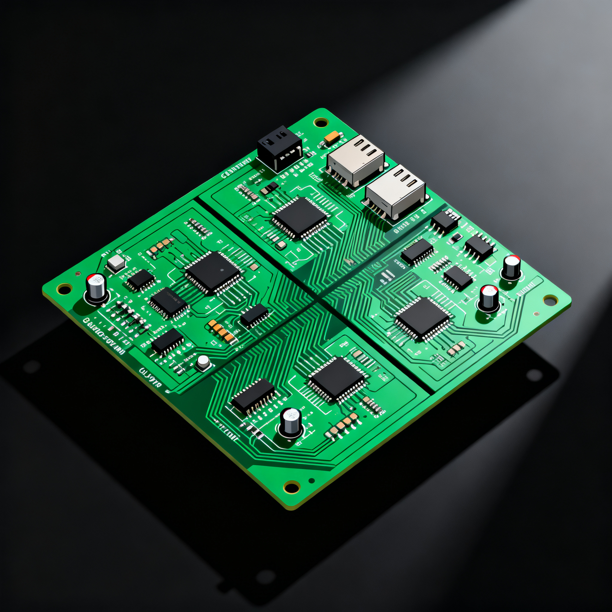
How to Design and Assemble a 4-Layer Audio Main Control Board with Split Ground Planes and Low-Noise Mixed-Signal Routing
How to Design and Assemble a 4-Layer Audio Main Control Board: Split Ground Planes and Low-Noise Mixed-Signal Routing Why Audio Main Boards Fail Silent: The Cost of Noisy Grounds and Poor Assembly An ...
How to Design and Assemble a 4-Layer Audio Main Control Board: Split Ground Planes and Low-Noise Mixed-Signal Routing
Why Audio Main Boards Fail Silent: The Cost of Noisy Grounds and Poor Assembly
An audio main control board that hums, pops, or drops a channel after six months in the field isn't just an annoyance — it's a liability. Product‑liability case law has long recognized that design and manufacturing defects that cause a product to malfunction can lead to costly recalls and legal exposure (Thomson Reuters, 2025 ed.). When the root cause traces back to a ground bounce on a split plane or a plating void inside a via, the OEM pays for it twice: once in re‑work and a second time in reputation.
The silent killer in mixed‑signal audio boards isn't usually a gross short. It's the intermittent, temperature‑dependent behavior that escapes final test. A 3D X‑ray system can reveal internal particles, sealing‑lid voids, and BGA/QFN joint abnormalities that thermal cycling or flying‑probe test never catch (Matric). Meanwhile, common plating voids — air bubbles, poor catalyzation, insufficient hole cleaning — create high‑resistance paths that generate noise and eventually fail open (MCL). Even large‑scale electrical infrastructure carries the same lesson: the infamous Federal Pacific, Zinsco, Challenger, and Pushmatic panel recalls proved that grounding and connection integrity are safety and performance fundamentals (MAS Pro Service). Audio control boards are no different; splitting a ground plane without rigorous fabrication control is like installing a recalled breaker panel — it may work for a while, but eventually it fails.
Tip: Demand a post‑etch AOI report and cross‑section coupon specifically through the gap region of your split plane. At NovaPCBA, we routinely supply these as part of the first‑article package for mixed‑signal boards.
How a 4-Layer Audio Stackup and Mixed-Signal Plane Architecture Actually Lower Noise
The physics is simple: every signal needs a return current. On a two‑layer board, that return flows through whatever copper pour it finds, often following a tortured path that couples digital noise into analog stages. A 4‑layer board with dedicated reference planes shortens the return loop and, crucially, lets you isolate analog and digital returns — provided you do it with discipline.
The classic 4‑layer audio stackup puts the ground split on layer 2, directly beneath the top‑side critical traces. Layer 3 carries power islands, and layer 4 is a second routing layer for low‑speed signals. This arrangement places the tightest signal‑reference coupling where it matters most. The standard board thickness is 1.6 mm (62‑mil), which gives good mechanical stiffness and is universally supported by fabrication shops (PCBvibe). For impedance‑controlled audio interfaces (like I²S running at a clean 50 Ω), the prepreg between L1 and L2 can be adjusted without changing the overall board thickness.
| Layer | Function | Material / Notes |
|---|---|---|
| L1 (Top) | High‑speed signal: I²S clocks, audio data, critical analog traces | 1 oz Cu, controlled impedance where needed |
| Prepreg | 0.10–0.15 mm (4–6 mil) for tight coupling | High‑Tg FR‑4, low Dk variation |
| L2 (Ground) | Split analog/digital ground with a single 3‑mm‑wide bridge at the ADC/DAC | 1 oz Cu; gap 0.25–0.40 mm (10–16 mil) |
| Core | ~0.50 mm | FR‑4 |
| L3 (Power) | Segmented power islands: AVDD, DVDD, Vcore | 1 oz Cu; pour with stitch‑vias to L2 |
| Prepreg | ~0.20 mm | FR‑4 |
| L4 (Bottom) | Low‑speed control: I/O, display, user interface | 1 oz Cu |
The split on L2 isn't arbitrary. You define an analog region for the codec, filters, and pre‑amps, and a digital region for the DSP, memory, and fast logic. The two regions meet at a single, wide copper bridge — a star point — directly underneath the mixed‑signal converter. This forces digital return currents to complete their loop inside the digital ground region without wandering into the analog domain. However, a split that is too wide, or a bridge that is too narrow, turns the gap into a slot antenna. If any digital trace crosses the split, the return current must detour around the gap, creating a large loop and coupling noise into everything nearby. The rule is absolute: never route a high‑speed trace over a split ground (Suga‑PCBA).
A well‑executed 4‑layer architecture supports audio amplifiers with signal‑to‑noise ratios better than 100 dB by keeping the analog ground "quiet" and confining switching noise to the digital region (Aivon tutorial on return‑path discipline). The key enabler is the continuous reference plane under every critical signal; any layer transition must immediately re‑establish that reference with a stitching capacitor or a pair of vias, as emphasized by Suga‑PCBA's continuous‑reference requirement. Without it, the return current jumps to the nearest copper and contaminates the analog plane.
4-Layer vs. 6-Layer for Audio Main Control Boards: When Adding Layers Makes Financial Sense
The decision between a 4‑layer board with a split ground and a 6‑layer board with two solid, contiguous reference planes isn't purely a technical one. It's a financial equation that includes development re‑spins, shielding costs, and line yield. Splitting a ground plane on a 4‑layer board introduces a demonstrable EMI risk; QueenEMS notes that the split can radiate and couple noise in ways a solid plane avoids, making a 6‑layer stackup the safer choice when EMI compliance is critical (QueenEMS).
| Comparison Metric | 4-Layer Board with Split Ground | 6-Layer Board with Solid Planes | Selection Criteria & Failure Boundary |
|---|---|---|---|
| Material & fab cost (1k units) | ~15–25% lower than 6‑layer; panel efficiency gains can reduce cost further (a 5 mm board shrink cuts per‑unit cost 15%) (WonderfulPCB) | Higher base cost, but more routing channels may shrink the board, offsetting some delta. | Choose 4‑layer if the design is tightly constrained and panel utilization is high. |
| Lead time (standard) | 7–10 days from Chinese manufacturers (WonderfulPCB); rush service costs 2–3× more. | Similar lead times for standard 6‑layer, but often 1–2 days longer due to extra lamination cycles (Aivon 2‑vs‑4‑layer). | Both fit standard quick‑turn if stacking is symmetrical and via depth is manageable. |
| EMI risk | High: split gap can radiate if digital traces cross the split or bridge is poorly sized. | Low: solid reference planes provide uninterrupted return paths. | If emissions testing is a known pain point, 6‑layer often avoids expensive shielding cans and common‑mode chokes. |
| Routing headroom | Two signal layers force tight spacing; mixed‑signal areas often congest. | Four signal layers give abundant space for isolation and length‑matching. | When more than 40 % of board area mixes analog and digital, routing on 4‑layer becomes a time sink. |
| Assembly touch time & rework | Higher: split‑plane issues often lead to more probing and manual tweaks at ICT, inflating cost. Additional special processes (e.g., VIPPO) raise unit price (TopFastPCBA). | Lower: solid planes reduce assembly quirks; standard via‑in‑pad options available. | Include debug and yield loss in the total cost of ownership; CMs report 10–15% longer test cycles on split‑ground 4‑layer audio boards. |
| Lifecycle cost (respin, shielding, field returns) | Can match or exceed 6‑layer if split‑plane EMI forces re‑spins or adds shielding. | Higher initial NRE, but typically fewer integration surprises. | For a product shipping >5k units, the 6‑layer premium often disappears after the first production run. |
The rule of thumb from seasoned audio designers: if your layout forces more than 40% of the board area to mix analog and digital regions with crossed return paths, the 6‑layer solution pays for itself in reduced debug and faster time‑to‑market. The cost of a single re‑spin — tooling, engineering time, delayed launch — dwarfs the delta in bare‑board price. Nevertheless, a well‑disciplined 4‑layer design with a properly sized split and careful routing can deliver production‑ready audio boards that pass EMC first pass, and many high‑volume consumer products still use this approach.
Routing Traps and Assembly Checks That Keep an Audio Board’s Noise Floor Intact
You’ve committed to a split ground. Now the execution determines whether the board measures –110 dB THD+N or radiates a 50 mV digital whistle into the analog path. The following rules — born from countless debug sessions — keep the noise floor where it belongs.
- Route every critical analog trace over its own un‑broken ground region. If a differential I²S line or a sensitive ADC input must change layers, place a stitching capacitor (100 nF directly between the reference planes) within 2 mm of the transition via pair.
- Keep the split bridge wide and short. A copper tie 3 mm wide by 2 mm long on 1 oz copper gives a DC resistance below 1.5 mΩ, but skin effect pushes its impedance up at noise frequencies. Simulate the bridge in a 2.5D field solver and never neck it down to less than 1.5 mm.
- Avoid slot‑antenna geometries. Never run a trace along or across the ground gap. Even guard traces left floating act as parasitic antennas.
- Specify ENIG finish for the entire board. A flat, corrosion‑resistant surface eliminates the oxide rectification that turns a solder joint into a noise generator. In the analog region, plugged and capped vias‑in‑pad (VIPPO) prevent flux entrapment and long‑term leakage currents.
- Validate fabrication quality early. Insufficient hole cleaning and poor catalyzation create plating voids that behave like tiny open circuits, generating bursts of noise when thermal expansion shifts them (MCL). Request a cross‑section coupon through the split gap and measure isolation resistance >100 MΩ at flying‑probe.
- Use 3D X‑ray for BGA and QFN hidden joints. Real‑time or film X‑ray may miss subtle head‑in‑pillow defects; only 3D X‑ray can verify complete solder coalescence under a DSP or large codec (Matric). At NovaPCBA, we employ X‑ray inspection on 100% of boards with mixed‑signal BGAs.
- Shrink the board smartly to save cost. Reducing the outline by just 5 mm can cut per‑unit cost 15% from better panel utilization (WonderfulPCB), but never at the expense of the split‑plane isolation. Use the freed board real estate to enlarge the ground bridge, not to pack parts tighter.
A table of assembly process parameters clarifies how each step directly affects the audio noise floor.
| Process Step | Key Quality Metric | Impact on Noise Floor | Verification Technique |
|---|---|---|---|
| Hole wall activation & copper plating | No voids, continuous 20 µm Cu in bore | Voids create high‑resistance returns → sporadic noise spikes | Cross‑section coupon, flying‑probe loop resistance |
| Solder mask application | Mask aligned to gap edges; <50 µm misregistration | Mask slivers across the gap create leakage paths | AOI, IPC‑TM‑650 isolation test |
| Surface finish (ENIG) | Gold thickness 0.05–0.12 µm, Ni 3–6 µm; Ra <0.4 µm | Rough or oxidized pads cause micro‑arcing noise at low signal levels | Profilometry, solderability test |
| Via filling (VIPPO) | Fully filled, no dimples >50 µm | Trapped flux outgassing leads to leakage and corrosion over 10‑year life | X‑ray, cross‑section, thermal stress test |
| BGA/QFN assembly & reflow | Void <25% per joint in X‑ray; complete coalescence | Intermittent joints cause digital glitches that couple into analog | 3D X‑ray, shear test on coupon |
| Split‑plane gap verification | Gap width per design ±30 µm; no copper slivers | Narrowed gap or sliver increases capacitive coupling between domains | Post‑etch AOI, cross‑section, TDR |
These checks aren't optional for a mixed‑signal audio board destined for professional or automotive use. The difference between a noise floor of –90 dB and –110 dB often lives in the copper‑to‑copper gap tolerance and the cleanliness of a single via. Following the return‑path discipline outlined in Aivon’s practical 4‑layer tutorial (Aivon) and the continuous‑reference warnings from Suga‑PCBA (Suga) gives the assembly staff a fighting chance to build a quiet board.
What Experienced Engineers and Buyers Ask Before Approving a Mixed-Signal Audio Board Design
Q: When does splitting the ground plane on a 4‑layer board do more harm than good?
A: The moment a high‑speed digital return path must cross the split, or the bridge between domains is thinner than 1.5 mm. A split only works when all noisy digital traces remain strictly over their own ground region and the analog section handles signals below a few hundred kHz. If your DSP communicates with an external memory bus that meanders across the board, the split becomes a slot antenna radiating harmonics into the analog domain. In that scenario, a 6‑layer board with a solid ground plane and partitioned power islands is the cleaner, lower‑risk solution.
Q: How do I calculate the optimal bridge width for the analog‑digital ground tie?
A: Target a bridge impedance below 0.1 Ω at the highest frequency of concern (usually the DSP core clock or a switcher harmonic). A copper trace 3 mm wide by 2 mm long on 1 oz copper yields about 1.5 mΩ at DC, but skin effect pushes the AC resistance up above a few MHz. Simulate the exact geometry in a 2.5D solver (e.g., Ansys Siwave or Keysight ADS) and place the bridge physically at the ADC/DAC — never at the I/O connectors — so that mixed‑signal return currents see the lowest possible inductance back to the source.
Q: Is a 4‑layer board with split planes actually cheaper than a 6‑layer after accounting for assembly yield and rework?
A: On bare‑board material alone, yes — typically 15–25% cheaper. But the total lifecycle cost often flips. Split‑plane EMI frequently forces the addition of shielding cans, common‑mode chokes, and ferrite beads that a solid‑plane 6‑layer board wouldn't need. Many contract manufacturers report that mixed‑signal 4‑layer boards require longer in‑circuit test cycles and more manual rework, shrinking the apparent cost gap to single digits. If even one field‑return campaign is triggered by intermittent ground‑bounce, the 6‑layer board is immediately the less expensive choice.
Q: What surface finish and via treatment best preserve low noise over a 10‑year lifetime?
A: ENIG (electroless nickel immersion gold) is the preferred finish: it yields a flat, corrosion‑resistant surface that prevents the oxide rectification effect that generates low‑frequency noise in humid environments. In the analog region, specify plugged and capped vias in pad (VIPPO) to eliminate flux entrapment and moisture ingress paths that degrade inter‑trace resistance over years. Avoid OSP on mixed‑signal audio boards; the thin organic film offers no protection against micro‑arcing at low signal levels.
Q: How do I verify that my PCB fab has executed the split plane gap correctly and not left copper slivers?
A: Start with a post‑etch automated optical inspection (AOI) report of the entire ground plane layer, and supplement it with a cross‑section coupon cut exactly through the split region. For mid‑ to high‑volume runs, add test pads on each side of the gap (one on analog ground, one on digital) and measure isolation resistance at the flying‑probe stage — you want >100 MΩ at 100 V. A TDR pulse across the gap also reveals any narrowing or slivers that increase capacitive coupling.
Q: For an audio main board with a DSP and codec, can I still use a 2‑layer board if my volumes exceed 100,000 units?
A: It’s possible but rarely robust. A 2‑layer board would need thick copper pours and meticulous star grounding, which often forces a larger board outline to provide enough isolation. At 100k volumes, the per‑unit delta between a large 2‑layer board and a compact 4‑layer board shrinks dramatically because panel utilization improves. A 2‑layer design also requires hand‑tuning of ground loops and may not deliver the repeatable noise performance needed for production consistency. The 4‑layer board removes those variables, making it the smarter choice for high‑volume, high‑reliability audio products.
References & Further Reading
- Product Liability: Design and Manufacturing Defects, 2025-2026 ed. | Thomson Reuters
- How to Address PCB Failures Effectively - Matric Blog
- PCB Issue Guide: PCB Failure Analysis and Common Issues - MCL
- Electrical Panel Recall List Homeowners Should Know About - MAS Pro Service
- 4 Layer vs 6 Layer PCB: The Ultimate Cost & EMI Guide - QueenEMS
- 4-Layer PCB Manufacturing and Stack-up - Wonderful PCB
- 2-Layer vs 4-Layer FR4 PCB: Cost, Performance, and Design Differences - Aivon
- How Much Does a 4 Layer PCB Cost? Cost Factors Explained - TopFastPCBA
- Mastering 4-Layer PCB Design: A Comprehensive Guide to Layout & Stackup - Aivon
- Complete PCB Layer Stackup Design Guide for 4 Layer Board - PCBvibe
- 4 Layer PCB Guide: Layers, Stackups and Design Choices - Suga-PCBA
- 4 Layer PCB Stack Up: A Practical Tutorial for Simple Designs - Aivon
Conclusion
Designing and assembling a 4‑layer audio main control board with split ground planes is a tightrope walk between cost and performance. When you respect the return‑current physics, enforce a single low‑impedance bridge at the mixed‑signal converter, and validate every step from plating to final X‑ray, the result is a production‑ready board with a noise floor that rivals far more expensive constructions. For projects where the analog‑digital partition is clean, the 4‑layer approach remains a workhorse. For everything else, the cost of a 6‑layer board with solid planes pays itself back in the form of one‑pass EMC and zero field‑return headaches. At NovaPCBA, we combine advanced AOI, 3D X‑ray, and cross‑section analysis to ensure that your mixed‑signal audio board meets its noise specification from the first prototype to the 100,000th unit.