How to Design a Custom 4-Layer PCB Assembly: A Step-by-Step Guide for Engineers
Why a Custom 4‑Layer PCB Assembly Demands Attention Right Now What used to be a niche, high‑speed luxury is now a baseline for countless new designs. Four‑layer PCBs are appearing in industrial IoT co...
Why a Custom 4‑Layer PCB Assembly Demands Attention Right Now
What used to be a niche, high‑speed luxury is now a baseline for countless new designs. Four‑layer PCBs are appearing in industrial IoT controllers, medical wearables, and even cost‑sensitive consumer gadgets where signal integrity and compact form factors matter. But the landscape has shifted. FR‑4 and copper‑clad laminate shortages—persisting through 2026—have forced engineering teams to move beyond “set and forget” material choices (PCB Material Shortages in 2026). Procurement now runs in parallel with layout: you must review BOM risk continuously, not just at part selection, and be ready to swap laminates in days, not weeks.
At the same time, field failures carry heavier consequences than ever. A single PCB defect can cascade into production stops, warranty claims, or product recalls that disrupt entire supply chains (6 Common Causes of PCB Failure). For a custom 4‑layer assembly, the margin for error shrinks: a poorly chosen stackup, an uncontrolled impedance mismatch, or a missed DFM rule can turn a promising design into a costly re‑spin. That’s why a step‑by‑step approach—from stackup planning through manufacturing handoff—is no longer optional. It’s how experienced engineers bridge the gap between a clever schematic and a reliable, production‑ready board.
The Anatomy of a 4‑Layer Stackup—Signals, Planes, and Prepregs Explained
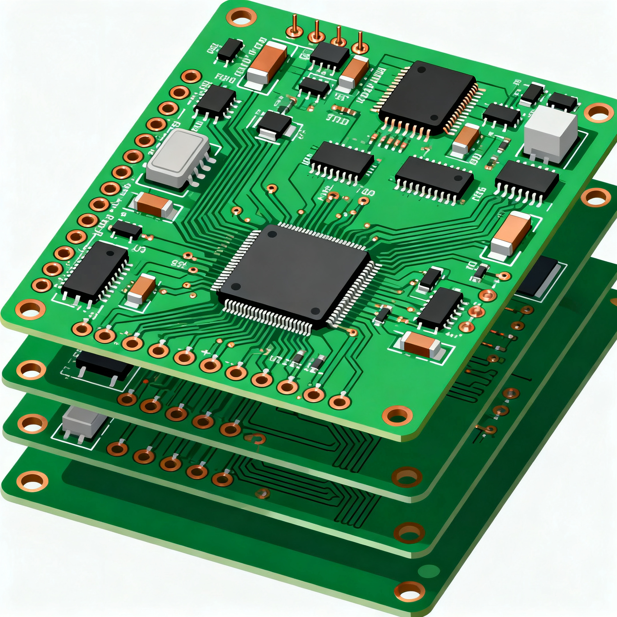
At its core, a 4‑layer PCB sandwiches four copper foils separated by insulating dielectric layers. The most common architecture arranges these as Signal‑Ground‑Power‑Signal (S‑G‑P‑S), with the top and bottom layers dedicated to routing, while the inner two form a solid ground plane and a power plane (Mastering the PCB Fabrication Process). This pairing isn’t just about real estate—it delivers a continuous return path directly adjacent to every signal layer, drastically reducing loop inductance and crosstalk.
The plane pair also creates inherent capacitance. When a high‑speed logic edge switches, the ground‑power sandwich acts as a distributed decoupling element, lowering the impedance of the power delivery network (PDN) at higher frequencies. But that benefit hinges on picking the right dielectric thickness and material. If you increase the core thickness to stiffen the board, you lose plane capacitance and may introduce unwanted resonances. Conversely, a very thin prepreg between power and ground can cause field‑coupled noise to bleed into other layers if not properly bypassed.
| Stackup Parameter | Typical Value/Range | Unit & Notes |
|---|---|---|
| Layer order (S‑G‑P‑S) | Top Signal – Ground Plane – Power Plane – Bottom Signal | Most common for general‑purpose digital/analog |
| Alternative (G‑S‑S‑G) | Ground – Signal – Signal – Ground | Used when inner signal layers need shielding |
| Core material (inner layers) | FR‑4, Tg 135–180 °C | Higher Tg for lead‑free reflow; matched CTE with prepreg |
| Prepreg type | 2116, 7628 glass weave; resin content ~45–55% | Thinner prepreg reduces loop inductance but can suffer from weave skew |
| Dielectric constant (Dk) @ 1 GHz | 4.2–4.8 (standard FR‑4); 3.8–4.2 (low‑Dk) | Lower Dk reduces trace capacitance; essential for controlled impedance above 1 GHz |
| Dissipation factor (Df) @ 1 GHz | 0.015–0.025 (standard); 0.005–0.010 (low‑loss) | Affects signal attenuation on long high‑speed traces |
| Copper weight (outer/inner) | 1 oz (35 µm) outer; 0.5 oz (18 µm) or 1 oz inner | Planes often 0.5 oz for fine line resolution; heavier copper for power electronics |
| Total board thickness | 1.6 mm (standard); 0.8–1.0 mm for compact designs | Thinner stackups improve heat dissipation but may warp during reflow |
| Impedance control target | 50 Ω single‑ended; 100 Ω differential | Achieved by adjusting trace width/space and dielectric height; fab must verify with coupons |
The stackup you choose must be drafted inside your EDA tool before any trace is laid. In Altium Designer, for example, you define the layer stackup and assign materials, then let the impedance calculator adjust geometries based on the manufacturer’s actual Dk and thickness values (Arshon’s complete guide). Failing to lock in the stackup early is the single largest source of post‑layout rework: if the fabricator later substitutes a different prepreg, your carefully tuned differential pairs may shift out of spec, adding weeks of delay.
Prototype Fab or Volume Production? Cost and Lead‑Time Trade‑Offs for 4‑Layer Boards
The moment you have a schematic and a preliminary stackup, you face a sourcing decision: do you order five quick‑turn prototypes from an overseas online service, or engage a domestic manufacturer that can eventually ramp to production? The answer depends on where you are in the development cycle, your tolerance for engineering support gaps, and how much you value the ability to amortize NRE.
Online prototype services have drastically narrowed the price gap for 4‑layer boards. As noted by PCBSync, some overseas fabs now offer 4‑layer prototypes at prices approaching those of 2‑layer boards, albeit with slightly longer lead times (PCBSync’s stackup vs. cost insight). If you only need a handful of boards for bring‑up, the unit price might be as low as $5–10 each—but that price rests on panelisation, minimum specs, and limited material options. For a production run of 500 pieces, however, custom manufacturers often undercut the “advanced” tier of budget fabs once HDI features or tight impedance control enter the picture (AtlasPCB’s JLCPCB vs. custom manufacturer analysis).
Quoting volatility comes from hidden cost drivers: NRE charges for electrical test fixtures, laser‑drilled via premiums, and the impact of surface finish selection. A quote that assumes flying‑probe testing and HASL finish can be 20–30% lower than one with bed‑of‑nails testing and ENIG—yet those differences directly affect long‑term reliability. The rule of thumb from the pricing guide by PCBAndAssembly holds true: “upload your Gerber files—most online quoting engines provide a real‑time price that updates as you adjust parameters” (PCBAndAssembly’s pricing guide). But an instant quote means little if stackup, tolerances, and testing aren’t aligned. TopfastPCBA emphasizes that the most useful comparison is not “Which supplier is cheaper?” but “Are both quotations based on the same engineering requirements?” (TopfastPCBA’s cost factors).
| Comparison Metric | Online Quick‑Turn Prototype (e.g., JLCPCB, PCBWay) | Domestic/Regional Custom Fab | Full‑Service EMS Partner |
|---|---|---|---|
| Typical order volume | 5–50 pcs | 50–5,000 pcs | 500+ pcs with full box‑build |
| Unit cost (4‑layer, standard FR‑4) | $5–15 (prototype); $3–8 at 500 pcs | $8–25 at 500 pcs, depending on testing and finish | $12–30 per assembly, including component sourcing and ICT |
| Lead time | 3–7 days (expedited); 2 weeks typical | 2–4 weeks with DFM review | 4–8 weeks, but includes full BOM risk analysis |
| Impedance control | Available at premium; may use standard coupons without TDR | Includes impedance coupon & TDR report; better tolerance control | Full signal integrity support and iterative stackup optimization |
| DFM feedback | Automated rule check only; minimal human engineer review | Detailed CAM review with suggested adjustments | Joint design‑for‑manufacturing workshops before tape‑out |
| Lamination change flexibility | Limited to in‑stock materials; substitutions may occur without notification | Proactive alerts when material is on allocation; offers validated alternatives | Manages alternative laminate qualification and builds test vehicles |
| When to choose | Early bring‑up, proof‑of‑concept, low‑complexity boards | Pre‑production validation, mid‑volume OEM builds | Products requiring IPC Class 2/3, full traceability, and ongoing demand |
Choosing the right partner for the phase you’re in is as much a schedule decision as a cost one. An online prototype order that arrives in a week might accelerate firmware development, but if the stackup you tested can’t be replicated in production because the high‑volume fab uses a different prepreg, you’ve just traded short‑term speed for a later re‑qualification headache. Factor in the supply‑chain reality described earlier—laminates go on allocation—and the need for early, transparent collaboration with your chosen manufacturer becomes unmistakable.
Designing for Manufacturability: Rules and Pitfalls That Prevent Field Failures
A 4‑layer board that works on the bench but fails after 50 thermal cycles often suffers from design‑induced stress, not component defects. The step‑by‑step process from schematic to Gerber generation is where you embed reliability. Start with a verified schematic; use your EDA tool’s library to place and interconnect components, then define the layer stackup before routing a single trace (Arshon’s guide). A common mistake is leaving plane definition until after routing, which forces compromises in return paths.
Once the stackup is set, follow these concrete DFM rules, tempered by field experience:
- Trace‑to‑plane clearance and impedance: For a 50 Ω single‑ended trace on a standard 1.6 mm 4‑layer board (S‑G‑P‑S), a 6‑mil trace with 4‑mil spacing over the ground plane on the top layer might yield 50 Ω if the dielectric between top copper and the ground plane is ~4 mil. Re‑calculate with your fabricator’s exact Dk.
- Via anti‑pad and thermal relief: Don’t place vias directly under tall components without checking soldermask clearance. Use thermal relief spokes (8‑10 mil spoke width) on inner plane connections to prevent cold joints during assembly, while maintaining enough copper to carry current.
- Split planes and return paths: Never route a high‑speed signal across a split in the ground plane. The return current will detour, creating loop area and EMI. If you must use a split analog/digital ground, keep the gap narrow and bridge it with a single point near the mixed‑signal IC, then route signals over the uninterrupted region.
- Mixed‑signal layout: Place analog front‑end circuits as far as possible from switching regulators and high‑speed buses. Use the power plane as a shield for sensitive analog traces by routing them on the bottom layer immediately beneath the continuous ground plane.
- Component placement sequence: Place connectors, mounting holes, and critical analog blocks first. Then position decoupling capacitors as close as possible to IC power pins—on the same side, with the via to the power plane directly in the pad if manufacturable.
The pitfalls table below captures the most frequent oversights that lead to field failures, along with the thresholds that separate a robust design from a marginal one (JHYPCB’s design guidelines and MorePCB’s 4‑layer walkthrough).
| Design Rule | Recommended Value / Practice | Pitfall if Ignored |
|---|---|---|
| Annular ring on vias | ≥5 mil (outer layers); ≥4 mil (inner) | Drill breakout leads to open circuits and intermittent connects |
| Through‑hole pad to inner plane clearance | ≥8 mil anti‑pad diameter larger than hole | Shorts to plane during soldering or reduced insulation resistance |
| Soldermask sliver width | ≥4 mil between pads | Slivers peel during assembly and create solder bridges |
| Trace spacing for high‑voltage | Use IPC‑2221 creepage tables; for 100 V, ≥40 mil on outer layers | Arcing across contamination on the board surface |
| Plane voiding under signal vias | Anti‑pad in ground plane symmetrically around via barrel | Stub resonance at high frequencies, degrading signal integrity |
| Copper balance across layers | Copper density variation <10% across the panel | Warpage during reflow, especially with thin cores |
| Silkscreen over pads | Clearance of at least 4 mil | Solderability issues and misleading DRC approvals |
After routing, run a thorough design rule check (DRC) with a ruleset that matches your manufacturer’s capabilities. Generate Gerber files, a drill file, and a fabrication drawing that spells out stackup, controlled impedance notes, and material preferences. The fab drawing is your contract—ambiguity there is the root cause of many “it passed DRC but the board doesn’t work” scenarios.
Perhaps the most overlooked step is early collaboration with the assembly house. Even if you’re still in layout, sharing a preliminary placement and stackup can uncover thermal issues, test access constraints, or component‑lead‑time problems that render a perfect board unbuildable. The supply‑chain events of the last year underscore this: a single end‑of‑life capacitor can force a schematic change that propagates into the PCB artwork—and the sooner you know, the less rework you’ll endure.
Questions Every Engineer and Buyer Should Ask Before Finalizing a 4‑Layer Assembly
Q: When does a 4‑layer board outperform a carefully laid‑out 2‑layer design?
Four layers become necessary when return‑path discontinuities, crosstalk, or EMI can’t be tamed with a single ground plane. If your design exceeds ~50 MHz, uses high‑speed digital buses, or mixes sensitive analog with fast switching, the dedicated power‑ground plane pair of a 4‑layer stackup dramatically lowers inductance and isolates signals. Cost and board thickness are the trade‑offs, but modern PCB fabs have narrowed the price gap to the point where the engineering time saved often outweighs the unit cost delta.
Q: Which stackup should I choose: signal‑ground‑power‑signal or ground‑signal‑signal‑ground?
Signal‑ground‑power‑signal (S‑G‑P‑S) is the most common and cost‑effective for general‑purpose digital and analog designs. It puts signals on outer layers and tightly couples the power‑ground planes in the middle, providing good plane capacitance. The alternative G‑S‑S‑G is used when you need two shielded inner signal layers, often for differential pairs or when outer‑layer access is limited. Each has different impedance profiles—select based on routing complexity and EMI sensitivity, not just convention.
Q: At what point is controlled impedance mandatory, and how does it affect fabrication cost?
Controlled impedance is required for USB, PCIe, DDR memory, and RF traces where timing and signal integrity are critical. Fabricators achieve it by precisely controlling dielectric thickness and trace width. It adds cost because it demands tighter process tolerances, impedance coupons on the panel, and often TDR testing. For a 4‑layer board with a few differential pairs, the premium is typically 10–20 % over standard construction; for boards full of controlled traces, the delta can be higher. Always specify impedance requirements in the fab notes and verify with a calculator early.
Q: How do I evaluate a substitute laminate when my preferred core/prepreg is on allocation?
Start with the supplier’s IPC‑4101 slash sheet to compare Tg, Dk, Df, and CTE. Match the Dk and loss tangent as closely as possible, especially for high‑speed boards. Check if the substitute requires modified trace geometries to hit the same impedance. Then run a thermal reliability assessment—different resin systems can warp differently during reflow. Involve your assembly house early and test a small batch before committing to volume, as noted in the material‑shortage strategies from the supply‑chain context (Material‑shortage strategies).
Q: What’s the best way to compare quotes from different prototype PCB assembly vendors?
Ensure all quotes are based on identical Gerber data, stackup specification, surface finish (ENIG vs. HASL), solder mask color, and IPC class. Hidden differences often lie in panelisation, minimum hole size, annular ring requirements, and whether electrical testing is flying‑probe or bed‑of‑nails. The comparison section of this guide references resources that help you normalize quotes—upfront alignment on these engineering details prevents later surprises in price and lead time (PCBAndAssembly’s pricing guide, TopfastPCBA cost factors).
Q: Can I reuse a proven 2‑layer footprint library on a 4‑layer board without modification?
Yes, the physical footprints (pad sizes, distances) remain valid, but you must re‑evaluate thermal relief connections to inner planes and check that no buried vias or blind connections are inadvertently created if your 4‑layer design uses different via types. Also verify that your 3D models and keep‑out zones don’t clash with changes in board thickness. A quick DRC pass with the new stackup ruleset catches most issues.
Bringing it all together: A disciplined step‑by‑step workflow—grounded in a validated stackup, clear DFM rules, and early manufacturing engagement—is what turns a good 4‑layer design into a reliable product. Whether you’re navigating allocation‑driven laminate swaps or optimizing for production cost, the same principle holds: the more engineering effort you invest before tape‑out, the fewer surprises you face in the field. For teams that need a partner to carry a design from schematic review through volume assembly, NovaPCBA provides full‑turnkey support—combining DFM analysis, material risk mitigation, and assembly services so you can focus on your core IP. The result is a 4‑layer board that arrives on time, within budget, and ready to perform.
References & Further Reading
- PCB Material Shortages in 2026: R‑4 and Copper‑Clad Laminate
- 6 Common Causes of PCB Failure: What OEMs Should Know
- 4‑Layer PCB: A Complete Guide to Design, Fabrication, and Manufacturing – Arshon Inc.
- Mastering the PCB Fabrication Process: A Step‑by‑Step Guide to 4‑Layer Designs – NovaPCBA
- How to Design 4 Layer PCB: Complete Step‑by‑Step Guide – MorePCB