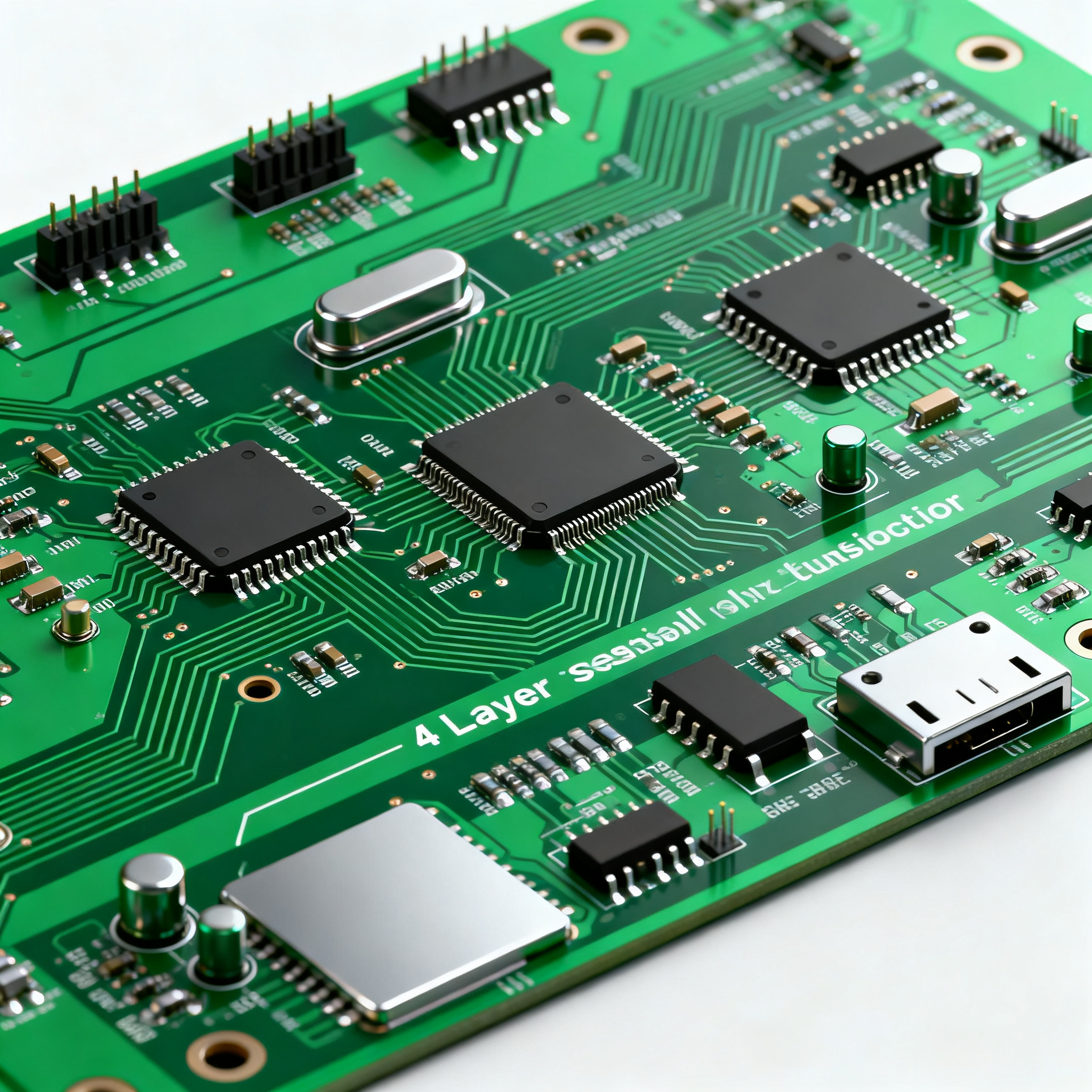
How to Design a 4-Layer Sensor Fusion PCB: A Step-by-Step Layout and Assembly Tutorial
Why Sensor Fusion PCB Designs Are Moving to 4 Layers—and the Layout Traps to Avoid Sensor fusion modules—combining inertial measurement units (IMUs), MEMS microphones, environmental sensors, and time-...
Why Sensor Fusion PCB Designs Are Moving to 4 Layers—and the Layout Traps to Avoid
Sensor fusion modules—combining inertial measurement units (IMUs), MEMS microphones, environmental sensors, and time-of-flight ranging chips—have become the sensory backbone of drones, wearables, robotics, and advanced driver-assistance systems. As these multi-sensor systems shrink, the traditional 2‑layer PCB quickly runs into a wall: digital noise from an SPI bus couples into an analog microphone trace, ground return paths meander, and the lack of a continuous reference plane turns even a slow I²C line into an EMI radiator.
Moving to a 4‑layer board solves most of these headaches by providing dedicated ground and power planes. But the migration isn’t a silver bullet. A poorly chosen stackup—say, placing the ground plane on layer 3 instead of layer 2—can still ruin signal integrity, and splitting the ground plane under a mixed-signal sensor often creates more problems than it solves. The cost of getting it wrong shows up late: intermittent sensor glitches, failed radiated emissions tests, or calibration drift that only appears after assembly.
This tutorial walks you through the entire design flow for a 4‑layer sensor fusion PCB, from stackup selection and mixed-signal partitioning to assembly with a partner like Nova PCBA. Along the way, we’ll highlight the layout traps that catch even experienced designers and show how to avoid them using proven techniques grounded in IPC‑2221 design standards.
Key Takeaways: A 4‑layer board with a signal‑ground‑power‑signal stackup gives you the low‑impedance return paths and isolation needed for reliable sensor fusion. But you must manage analog/digital partitioning, via stitching, and impedance targets carefully—otherwise the board will behave no better than a 2‑layer design.
The 4-Layer Stackup That Balances Signal Integrity and Mixed-Signal Isolation
The most widely used 4‑layer arrangement for sensor fusion is Layer 1 (top) – signals, Layer 2 – ground, Layer 3 – power, Layer 4 (bottom) – signals. This stackup places a continuous ground plane immediately beneath the top‑side components, providing the shortest possible return path for high‑speed digital edges and shielding analog traces from radiated noise. The power plane on layer 3 acts as a low‑inductance distribution layer and, together with the ground plane, forms a parallel‑plate capacitor that helps suppress power‑supply ripple.
When you route a mixed‑signal design, the golden rule is: do not split the ground plane. Instead, partition the board into analog and digital sections on the top layer and keep the layer‑2 ground plane solid. Route all analog signals over a quiet area of the ground plane, far from high‑speed digital buses. If a sensor requires a separate analog ground (AGND) and digital ground (DGND), tie them together at a single point directly under the sensor—never create a slot in the plane.
Return paths matter just as much. A high‑speed SPI clock edge on layer 1 will induce a return current on layer 2 directly beneath the trace. If that return current is forced to detour around a plane cutout or a dense via field, you get ground bounce and increased EMI. A continuous ground plane keeps the loop area small, which is critical for passing radiated emissions tests.
Impedance control, per IPC‑2221, is essential for interfaces like SPI (when clock rates exceed 10 MHz) and for differential pairs such as MIPI CSI‑2 or I²S audio. The table below shows typical trace geometries for a common 4‑layer stackup: 1.6‑mm total thickness, FR‑4 (εr ≈ 4.5), 1‑oz copper, with a 0.2‑mm prepreg between layers 1‑2 and 3‑4, and a 1.0‑mm core between layers 2‑3.
| Sensor Interface | Signal Type | Target Impedance | Trace Width (mil) | Spacing to Ground (mil) | Notes |
|---|---|---|---|---|---|
| I²C (100/400 kHz) | Open-drain, single-ended | Not critical | 10 | ≥ 10 | Wider trace reduces IR drop; no impedance control needed. |
| SPI (≤ 25 MHz) | Single-ended CMOS | 50 Ω ±10% | 12 | ≥ 10 | Route clock first, keep stubs short; series‑terminate at driver if needed. |
| Analog MEMS mic (PDM) | Single-ended analog | High‑impedance | 8 | Guard ring, 5‑10 mil gap | Surround trace with grounded guard ring on same layer; no impedance target. |
| I²S audio (up to 12.288 MHz) | Differential or single-ended | 100 Ω diff. / 50 Ω SE | 8 / 8 (diff. pair) | ≥ 10 to other pairs | Route as tightly coupled differential pair; length‑match within 50 mil. |
| UART (up to 3 Mbps) | Single-ended | 50 Ω optional | 10 | ≥ 8 | Low speed; prioritize routing convenience over impedance. |
| Analog sensor output (0‑3.3 V) | Single-ended low‑frequency | Not applicable | 8 | Guard ring, 5‑10 mil | Use star ground routing to ADC input; add RC filter close to ADC pin. |
These numbers assume a standard 0.2‑mm prepreg dielectric. If your fabricator uses a different material (e.g., a 0.1‑mm prepreg for tighter impedance tolerance), the trace widths will shrink—always verify with a field solver or your board house’s impedance calculator. The takeaway is that a 4‑layer stackup gives you enough control to hit 50‑Ω and 100‑Ω targets without resorting to impractically wide traces, while the solid ground plane keeps analog signals quiet.
When 4 Layers Beat 2 (and When They Don't) for Sensor Fusion
Not every sensor fusion board needs four layers. A simple combination of a temperature/humidity sensor and an ambient light sensor on a 2‑layer board can work perfectly if you follow careful layout rules. But as soon as you add a digital accelerometer/gyroscope (SPI), a MEMS microphone (analog or PDM), and perhaps a BGA‑packaged sensor hub, the limitations of a 2‑layer stack become expensive. The table below compares 2‑layer, 4‑layer, and 6‑layer options for typical sensor fusion designs.
| Comparison Metric | 2‑Layer PCB | 4‑Layer PCB | 6‑Layer PCB | Selection Criteria & Failure Boundary |
|---|---|---|---|---|
| Crosstalk isolation (adjacent traces) | Poor; no dedicated plane, ground pours easily fragmented | Good; continuous ground plane absorbs field lines | Excellent; multiple ground planes further reduce coupling | Use 4‑layer when analog sensitivity is < 1 mV or digital edge rates exceed 1 ns. |
| EMI radiated emissions margin | Often fails FCC/CISPR unless shielded | Passes with proper stackup; 6‑10 dB margin typical | Passes with > 10 dB margin; easier to contain high‑speed clocks | If product is unshielded and close to regulatory limits, 4‑layer is minimum. |
| BGA fan‑out (0.5 mm pitch) | Impossible without via‑in‑pad and blind vias | Possible with dog‑bone fan‑out and via‑in‑pad (filled & capped) | Easy; microvias and multiple signal layers simplify escape routing | For a single BGA sensor, 4‑layer works; for dense BGAs with > 200 I/Os, go 6‑layer. |
| Power integrity (number of rails) | One or two rails with wide pours; noisy | Dedicated power plane can be split for 2‑3 rails | Multiple dedicated planes; ideal for 4+ voltage domains | If sensors require 1.8 V, 3.3 V, and a clean analog 3.0 V, 4‑layer with split plane is sufficient. |
| Relative PCB cost (1× = 2‑layer baseline) | 1× | 1.4–1.7× | 2.0–2.5× | 4‑layer cost adder is justified by reduced debug time and higher first‑pass success. |
| Design complexity | Low; but layout iterations are high to fix noise | Moderate; requires impedance planning and stackup definition | High; needs advanced via structures and layer‑pair planning | Choose 4‑layer when your team has experience with controlled impedance; otherwise, invest in training. |
| Typical sensor fusion application | 2‑3 low‑speed sensors (temp, humidity, light) | 6‑axis IMU + MEMS mic + environmental sensor + BLE MCU | 9‑axis IMU + multiple cameras (MIPI) + radar + sensor hub processor | 4‑layer is the sweet spot for most consumer and industrial fusion modules. |
The decision matrix shows that 4 layers hit the sweet spot for the vast majority of sensor fusion designs. You get the isolation and impedance control needed for mixed‑signal coexistence without the cost and complexity of a 6‑layer board. However, if your design includes a high‑speed MIPI D‑PHY interface (1.5 Gbps per lane) or multiple isolated power planes for different sensor voltages, the dielectric thickness constraints of a 4‑layer stack may force you to 6 layers to achieve the required differential impedance and routing density. Similarly, a dense BGA with 0.4‑mm pitch will demand microvia technology that is more naturally implemented on a 6‑layer board.
A Step-by-Step Layout and Assembly Tutorial for Sensor Fusion PCBs
With the stackup chosen and the layer‑count decision made, it’s time to execute the layout. This walkthrough covers the critical steps from footprint placement to post‑assembly calibration, with an emphasis on design‑for‑manufacturing (DFM) rules that ensure a smooth transition to production with an assembly partner like Nova PCBA.
Step 1: Partition the Board Before Placing a Single Component
Draw imaginary lines on your board outline to separate analog, digital, and power‑supply sections. Place the noisiest digital devices—the microcontroller, SPI flash, and high‑speed interfaces—on one side. Keep sensitive analog sensors (MEMS microphone, precision ADC) on the opposite side, with the power management IC (PMIC) in between. This physical separation minimizes the need for guard traces and reduces the risk of digital return currents crossing analog areas.
Step 2: Floor‑plan the Sensor Footprints with Return Paths in Mind
Position each sensor so that its analog pins face the quiet zone. For a 6‑axis IMU in a LGA package, orient the device so the SPI lines exit toward the digital section, while any analog auxiliary inputs face the analog area. Place decoupling capacitors on the same layer as the sensor, directly adjacent to the power pins, with vias dropping straight to the power and ground planes. This keeps the high‑frequency current loop tiny.
Step 3: Route Critical Signals First, Guard Where Needed
Route the SPI clock and data lines as 50‑Ω traces on layer 1, referencing the ground plane on layer 2. Keep them short and avoid layer changes. For the analog microphone trace, run it on layer 1 with a grounded guard ring on both sides—this ring should be connected to the ground plane with vias every 5‑10 mm. Digital traces that must cross the analog section should be routed on layer 4 (bottom), using the ground plane as a shield. Never route a digital trace parallel to an analog trace on the same layer.
Step 4: Via Stitching and Plane Management
Stitch the ground plane to the bottom‑layer ground pours with a perimeter of vias spaced no more than λ/20 at the highest frequency of concern (typically 1‑2 GHz for edge rates). This creates a low‑impedance fence that suppresses board‑edge radiation. Under mixed‑signal components, add a few extra ground vias to ensure the return current can find the shortest path. If the power plane on layer 3 is split for multiple voltages, make sure no high‑speed trace on layer 4 crosses a split—the return current would have to detour, causing EMI and signal integrity problems.
Step 5: DFM for Fine‑Pitch Sensor Packages
Many sensor fusion boards use 0.5‑mm pitch BGA or LGA packages. The table below summarizes the DFM parameters you need to lock down with your fabricator and assembler. Following these rules avoids solder bridging, opens, and reliability issues.
| DFM Parameter | Recommendation for Sensor Fusion PCB | Standard / Notes |
|---|---|---|
| Minimum trace/space | 4 mil / 4 mil (0.1 mm / 0.1 mm) | Consult fabricator; 3 mil possible at added cost. IPC‑2221 design rules. |
| Via type for 0.5‑mm BGA | Via‑in‑pad, filled and capped (VIPPO) or dog‑bone with 0.2‑mm drill | VIPPO required for full array; dog‑bone acceptable for perimeter I/Os. IPC‑6012 Class 2 annular ring. |
| Solder mask clearance | 2 mil (0.05 mm) expansion from pad edge | Prevents mask‑on‑pad and bridging; confirm with assembler. |
| Stencil thickness | 4 mil (0.1 mm) for 0.5‑mm pitch; step‑down to 3 mil for 0.4‑mm pitch components | Laser‑cut stencil with nano‑coating improves release for fine apertures. |
| Surface finish for analog sensors | ENIG (electroless nickel immersion gold) for flatness; immersion silver for ultra‑low noise | ENIG provides excellent planarity for fine‑pitch; silver avoids nickel’s magnetic properties. Nova PCBA offers both. |
| Post‑assembly cleaning | Aqueous wash to remove flux residues, especially under low‑standoff sensors | Flux residues can absorb moisture and drift humidity sensor readings. |
| Calibration test points | Include 1‑mm diameter test pads on bottom layer for I²C/SPI bus access and analog test voltages | Enables in‑circuit calibration without probing fine‑pitch pins. |
Step 6: Stencil Design and Assembly with Nova PCBA
For mixed‑technology boards that combine 0.5‑mm pitch sensors with larger connectors, a step stencil is often necessary. Work with your assembly partner to define the stencil aperture geometry—rounded square apertures for BGA pads improve paste release. Nova PCBA’s engineering team can review your stencil design and recommend aperture reductions to prevent solder bridging on fine‑pitch components while ensuring adequate volume for larger passive components.
Step 7: Post‑Assembly Calibration and Verification
After reflow, sensor fusion boards require calibration to compensate for assembly‑induced offsets. Design your firmware to read raw sensor data over the I²C/SPI bus and apply calibration coefficients stored in onboard EEPROM. Mechanical stress from PCB mounting can shift accelerometer and gyroscope biases, so specify a relaxed mounting scheme (e.g., rubber grommets) or perform a post‑assembly six‑point tumble calibration. Collaborate with your assembler to define a calibration fixture that mates with the test points you designed in Step 5.
Sensor Fusion PCB Assembly: Questions Engineers and Buyers Ask
Q: How do I prevent digital noise from coupling into my analog MEMS microphone traces on a 4‑layer board?
Use a continuous ground plane on layer 2, route the analog microphone trace on layer 1, and surround it with a grounded guard ring connected to the plane with vias every 5‑10 mm. Keep all digital traces on layer 4 (bottom) so the ground plane acts as a shield. Avoid splitting the ground plane under the microphone or the ADC—instead, partition the board physically so that digital signals never cross the analog area. Add a ferrite bead on the microphone’s power rail to filter high‑frequency noise, and place the decoupling capacitor as close as possible to the sensor’s power pin.
Q: What are the critical DFM rules for BGA sensor packages with 0.5 mm pitch?
For 0.5‑mm pitch BGAs, use via‑in‑pad only if the vias are filled with conductive or non‑conductive epoxy and plated over (VIPPO). If you fan out with dog‑bone vias, maintain a minimum annular ring of 0.125 mm (5 mil) per IPC‑6012 Class 2. Solder mask clearance should be at least 0.05 mm (2 mil) to prevent mask‑on‑pad defects. A 4‑mil trace and space is typical, but always verify with your fabricator’s capabilities. For assembly, a 4‑mil stencil with nano‑coating and rounded square apertures minimizes bridging risk.
Q: What surface finish minimizes noise for precision analog sensor inputs?
ENIG (electroless nickel immersion gold) is the most common choice because it provides an exceptionally flat surface for fine‑pitch components and low contact resistance. However, the nickel layer in ENIG has magnetic properties that can introduce noise in ultra‑sensitive magnetometers or high‑impedance analog circuits. In those cases, immersion silver or OSP (organic solderability preservative) are preferred—immersion silver offers excellent conductivity without nickel, while OSP is the most economical but has a shorter shelf life. Evaluate the sensor’s sensitivity and your signal‑to‑noise budget before deciding. Nova PCBA can guide you through the trade‑offs based on your specific sensor mix.
Q: How do I ensure sensor calibration accuracy after assembly?
Design dedicated test points for in‑circuit calibration—1‑mm pads on the bottom layer that give access to the I²C/SPI bus and analog test voltages. Avoid placing mounting holes or stiffeners near MEMS sensors, as mechanical stress can shift offsets. Specify a post‑reflow cleaning step (aqueous wash) to remove flux residues that can affect humidity and gas sensors. Work with your assembly partner to develop a calibration fixture that automates the process: the fixture should power the board, communicate with the sensor hub, and apply known stimuli (e.g., a reference orientation for the IMU, a calibrated sound source for the microphone). Store calibration coefficients in non‑volatile memory on the board.
Q: When should I move from 4 to 6 layers for a sensor fusion design?
Move to 6 layers when you need multiple isolated power planes for different sensor voltages (e.g., 1.2 V, 1.8 V, 3.3 V, and a clean analog 3.0 V) that cannot be adequately partitioned on a single split plane. Also upgrade if your design includes high‑speed interfaces like MIPI D‑PHY (1.5 Gbps per lane) that require tight differential impedance control—the thicker dielectric between layers 2‑3 in a 4‑layer stack may force trace widths that are too wide to route densely. Dense BGA fan‑out with 0.4‑mm pitch or multiple large BGAs also benefits from the additional routing layers and microvia options that a 6‑layer stack provides. If your 4‑layer layout is becoming a puzzle of split planes and serpentine traces, it’s time to add layers.
Designing a 4‑layer sensor fusion PCB is a balancing act between signal integrity, manufacturability, and cost. By starting with a proven signal‑ground‑power‑signal stackup, partitioning the board early, and following DFM rules tuned for fine‑pitch sensors, you can avoid the most common pitfalls. When you’re ready to move from prototype to production, a partner like Nova PCBA brings the assembly expertise, surface finish options, and calibration support needed to turn your design into a reliable, high‑yield product. The jump from 2 to 4 layers is often the single most impactful decision you’ll make for sensor fusion performance—make it with confidence.
References & Further Reading
- IPC – Association Connecting Electronics Industries – IPC‑2221 and IPC‑6012 standards for PCB design and fabrication.
- Nova PCBA – Professional PCB assembly services, including fine‑pitch BGA, ENIG/immersion silver finishes, and calibration support.
- PCBWay Impedance Control – Online impedance calculator and stackup design guidelines.
- Ultra Librarian – CAD footprints and ECAD/MCAD integration for sensor components.
- Octopart – Electronic component search engine for sourcing sensors and passives.
- Analog Devices Design Tools – Precision sensor signal chain design and simulation resources.
- STMicroelectronics STM32CubeMX – Sensor fusion firmware configuration and pin planning.