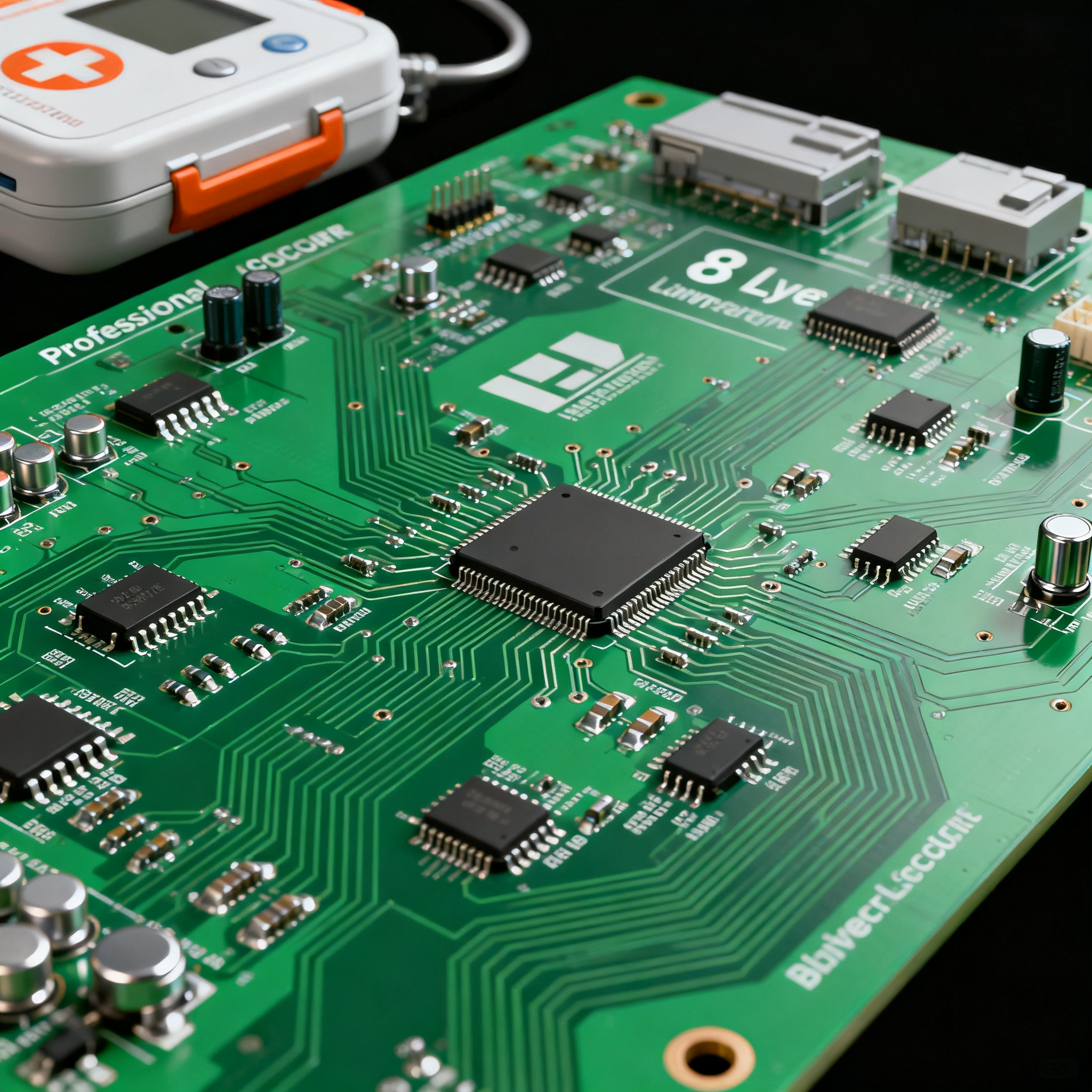
How to Achieve Medical-Grade Reliability in 8-Layer PCB Assembly: A Real-World Defibrillator Case Study
How to Achieve Medical-Grade Reliability in 8-Layer PCB Assembly: A Real-World Defibrillator Case Study The Silent Failure That Should Never Happen: Component Shortages, Substitutions, and the Defibri...
How to Achieve Medical-Grade Reliability in 8-Layer PCB Assembly: A Real-World Defibrillator Case Study
The Silent Failure That Should Never Happen: Component Shortages, Substitutions, and the Defibrillator’s Last Line of Defense
During a routine clinical audit, a portable defibrillator failed to deliver its therapeutic shock. The root cause was not a design flaw but a silent, systemic failure in the assembly supply chain. A procurement manager, facing a 52-week lead time on a critical high-voltage capacitor, had accepted a pin‑compatible substitute without re‑qualifying the entire signal path. The replacement part, while functionally identical on paper, introduced a slightly different leakage current characteristic that shifted the timing of the high‑voltage pulse. In a life‑or‑death moment, that shift was enough to render the device ineffective.
This is not an isolated incident. Component shortages pressure assemblers into substituting parts without notifying customers, and in medical applications, even a pin‑compatible alternative can alter electrical characteristics in ways that invalidate clinical performance. The reality is stark: there is zero tolerance for defects in life‑critical devices like defibrillators. A single hidden BGA defect or cold solder joint can lie dormant for years, only to fail when the patient needs the device most. That is why IPC Class 3 soldering and inspection are not aspirational targets—they are the baseline. Full traceability from bare laminate to final functional test is the only way to ensure that every component, every solder joint, and every process parameter can be traced back to a certified lot.
For an 8‑layer defibrillator board, the stakes are escalated by the high‑voltage, high‑current environment. An assembly error that might cause a nuisance trip in a consumer gadget can cause catastrophic failure in a defibrillator. That’s why the industry’s best‑in‑class manufacturers now build their entire quality management system around the assumption that any undetected deviation will eventually be exposed—and that exposure could be fatal.
Inside the 8-Layer Defibrillator PCB: Stack-Up Architectures and Dielectric Material Trade-offs
The defibrillator’s PCB must simultaneously manage three hostile environments: a 2‑5 kV charging circuit, a sensitive biopotential sensing front‑end, and a digital control section that demands low‑noise power delivery. An 8‑layer stack‑up is the minimum viable configuration that can provide the isolation, impedance control, and thermal management required for reliable operation. Defibrillator board design demands high‑voltage isolation, controlled impedance, and robust thermal management. The high‑voltage section must maintain creepage and clearance distances that prevent arcing across the board surface; the digital section needs tight impedance control on DDR memory busses; and the entire assembly must survive repeated thermal cycles without delamination.
Stack‑up architectures typically follow a symmetrical buildup to minimise warpage. A proven configuration starts with a high‑voltage isolation layer on the outer prepreg, followed by dedicated ground and power planes, then inner signal layers routed with buried striplines. The choice of dielectric material is pivotal. PCBWay’s medical design guide and PCBSync’s complete guide both emphasise that medical‑grade laminates must offer a high comparative tracking index (CTI), a glass transition temperature (Tg) well above 170°C, and a dielectric constant (Dk) that remains stable over temperature and frequency. The table below summarises the trade‑offs between the most common material families used in defibrillator PCBs.
| Material | CTI (V) | Tg (°C) | Dk @ 1 GHz | Typical Cost Multiplier | Best Suited For |
|---|---|---|---|---|---|
| Standard FR-4 | 175–225 | 130–140 | 4.2–4.5 | 1.0× | Low‑voltage digital sections (not recommended for high‑voltage isolation) |
| High‑Tg FR-4 (e.g., ISOLA 370HR) | 200–250 | 170–180 | 4.0–4.3 | 1.2–1.4× | General‑purpose medical, moderate voltage |
| Polyimide | 250–300 | 250–260 | 3.5–3.9 | 2.5–3.5× | High‑reliability, extreme thermal cycles |
| Ceramic‑filled Hydrocarbon (e.g., Rogers 4350B) | 400–600+ | 280 | 3.48 ± 0.05 | 4.0–6.0× | High‑voltage isolation, RF performance |
| PTFE‑based (e.g., Rogers 3003) | 600+ | 327 | 3.0 ± 0.04 | 6.0–8.0× | Microwave sensing, but poor adhesion and high cost |
Tip: For the defibrillator’s high‑voltage isolation layer, select a material with a CTI of at least 400 V. This ensures that the board can withstand the 2 kV pulse without surface tracking, even under the pollution degree 2 conditions typical of ambulance and hospital environments. Core assembly principles dictate that the same laminate should have a thermal conductivity of at least 0.5 W/m·K to dissipate the heat generated during rapid charging cycles.
The 8‑layer stack‑up also allows decoupling the high‑voltage ground from the sensitive analogue ground. By using dedicated internal planes, you can maintain a single‑point ground connection at the star point while keeping the return paths separated. This reduces common‑mode noise that could otherwise corrupt the ECG sensing front‑end. The result is a board that handles 2 kV pulses, ‑40 °C to +85 °C operation, and 10 years of shelf life—all within a footprint that fits inside a handheld defibrillator enclosure.
What Separates a Life-Saving Assembly Partner From a Commercial One: A Side-by-Side Look
Supplier selection for defibrillator PCBs is not about price alone. As Venture Manufacturing highlights, medical device PCB assembly demands quality consistency and process control that go far beyond the requirements of consumer electronics. A commercial assembler might deliver a perfectly functional board for a set‑top box, but the same process cannot guarantee the zero‑defect outcome needed for a Class III medical device. AdvancedPCB’s quick‑turn prototype services are valuable for validating designs early, yet they must be paired with a production partner that brings full‑scale traceability and medical‑specific process validations. PCBSync and SprintPCB Group stress the importance of real‑world case experience, cleaning and disinfection protocols, and creepage distance considerations that commercial shops rarely encounter.
To help you navigate the decision, the table below compares the capabilities of a typical commercial assembler, a medical‑focused EMS provider, and NovaPCBA’s zero‑defect, full‑traceability model built specifically for Class III medical assembly.
| Comparison Metric | Option A: Commercial Assembly | Option B: Medical Specialist (e.g., Venture/SprintPCB) | NovaPCBA Medical‑Grade Approach |
|---|---|---|---|
| Inspection Standard | IPC Class 2 (default), optional Class 3 | IPC Class 3 for all medical jobs | IPC Class 3 + in‑house 3D X‑ray on every board |
| Traceability | Batch‑level, paper‑based | Full lot traceability, digital records | Single digital thread: laminate lot to final test, real‑time audit access |
| Component Change Control | Informal substitution possible | Formal change notification, but may lag | Zero unauthorized substitution; OEM‑gated approval workflow |
| Prototype Validation | Quick‑turn, limited process data | Dedicated NPI line, process parameter capture | Full NPI with DOE on critical parameters, statistical process control |
| Cleanliness & Creepage | Standard wash, no IPC‑5704 compliance | Inline cleaning, ionic contamination testing | ISO 13485‑aligned cleaning, verified creepage/clearance per design audit |
The difference is not merely in the certificates hanging on the wall; it is in the engineering culture. A medical‑focused partner will have failure analysis engineers who understand the clinical consequences of a latent defect. They will ask about the defibrillator’s maximum energy delivery, the biopotential noise floor, and the expected shelf life before the first solder joint is even printed. That is the level of partnership a life‑saving device demands.
From IPC Class 3 to ISO 13485: The Regulatory Chain That Locks in Reliability
For a defibrillator PCB, the regulatory chain is not a paper exercise—it is the only proof that the board you are holding can be trusted with a life. IPC Class 3 solder joint standards and rigorous inspection are the entry point, but they must be woven into a broader quality system that includes ISO 13485 process validation. SprintPCB Group notes that cleaning protocols and creepage distances are audit‑critical, and QueenEMS emphasises full traceability to enable rapid failure analysis. The documentation trail must prove, with data, that every process step from incoming laminate to final automatic optical inspection (AOI) and X‑ray was executed within defined limits.
The following list maps the critical documentation nodes that an FDA auditor will expect to see for a Class III defibrillator assembly:
- Incoming Laminate: Certificate of Conformance (CoC) with lot number, Tg, CTI, and Dk values; ionic contamination test results.
- Inner Layer Imaging & Etch: First‑article reports with measured trace widths and impedance coupons; continuity test data.
- Lamination: Press cycle logs (temperature, pressure, time); microsection analysis of registration accuracy.
- Drilling & Plating: Hole wall quality reports; copper thickness measurements per IPC‑6012 Class 3.
- Solder Mask & Surface Finish: Mask adhesion test; ENIG/ENEPIG thickness verification; solderability test coupons.
- Assembly: Solder paste inspection (SPI) data for every pad; reflow oven profile with time‑above‑liquidus records; 3D X‑ray images for all BGA and QFN joints.
- Final Test: Functional test data including high‑voltage isolation at 150% of rated working voltage; boundary scan or flying probe reports; serialised test results linked to the board’s unique identifier.
The table below summarises the standards and verification methods that anchor each stage of the defibrillator PCB assembly process.
| Process Step | Applicable Standard | Verification Method | Acceptance Criteria |
|---|---|---|---|
| Laminate Selection | IPC‑4101, IPC‑TM‑650 | DSC for Tg, CTI per ASTM D3638 | Tg ≥ 170°C, CTI ≥ 400 V for isolation layer |
| Etch & Impedance Control | IPC‑6012 Class 3 | TDR measurements on impedance coupons | ±10% of nominal impedance |
| Solder Joint Quality | IPC J‑STD‑001 Class 3, IPC‑A‑610 Class 3 | AOI + 2D X‑ray (100%) + 3D X‑ray on BGAs | Zero voids > 25% of joint area, full fillet wetting |
| Cleanliness | IPC‑5704, ISO 13485 | Ionic contamination (ROSE) test | < 1.56 µg/cm² NaCl equivalent |
| High‑Voltage Isolation | IEC 60601‑1, IPC‑2221 | Hi‑Pot test at 150% rated voltage | No breakdown or flashover |
| Traceability | ISO 13485, FDA 21 CFR Part 820 | Digital thread audit | Full forward/backward traceability in < 4 hours |
When the FDA auditor asks for the lot history of the tantalum capacitor on the high‑voltage rail, you should be able to pull up the date code, the reflow profile it experienced, and the X‑ray image of its solder joints within minutes. That is the difference between a board that is merely assembled and one that is built to a medical‑grade reliability standard.
Defibrillator PCB Assembly: Questions Engineering Leads and Buyers Actually Ask
Q: What is the minimum creepage and clearance distance for a defibrillator PCB handling 2 kV pulses, and how does an 8‑layer stack‑up help achieve it?
IPC‑2221 requires at least 8 mm creepage for 2 kV with pollution degree 2, assuming an uncoated board. Clearance for the same voltage is typically 4 mm. An 8‑layer stack‑up allows you to dedicate internal planes as isolation barriers, routing high‑voltage tracks on inner layers where they are shielded from contamination. By using a buried stripline approach, you can maintain the required distance while keeping the board compact. The outer layers can then be used for low‑voltage signals, with the isolation layer’s CTI‑400+ material providing the necessary tracking resistance. SprintPCB’s experience with surgical equipment underscores that real‑world cleaning and disinfection protocols can degrade the surface, making internal routing of high‑voltage nodes the safer strategy.
Q: How can we ensure BGA solder joint integrity without X‑ray inspection on every board?
The short answer is: for a life‑critical defibrillator, you cannot skip 100% inspection of hidden joints. IPC Class 3 criteria demand a 100% X‑ray or an equivalent confidence method. In practice, the most defensible approach is to use 3D X‑ray on the first‑article board and then apply statistical process control (SPC) on the production line. Flying probe and boundary scan can supplement the inspection by catching electrical opens, but they cannot detect latent voids that will grow under thermal cycling. Hidden BGA defects are a known cause of post‑delivery failure, and the FDA will expect to see objective evidence that every BGA joint meets the voiding criteria. The most efficient path is to partner with an assembler that has in‑line 3D X‑ray capability and is willing to provide the images as part of the lot acceptance package.
Q: What traceability records do FDA auditors actually want to see for a defibrillator PCB assembly?
Auditors expect a single digital thread that connects the bare board laminate lot to the final functional test serial number. At a minimum, you must provide: laminate lot certificates and CTI test reports; solder paste lot number, date of opening, and SPI data for each board; component date codes and reel identifiers for all active and passive parts; reflow oven profile logs with time‑above‑liquidus; AOI and X‑ray images linked to each board’s unique identifier; and functional test results with pass/fail criteria. Full traceability enables rapid failure analysis; if a field return occurs, you should be able to isolate all boards built from the same component lot within hours, not weeks.
Q: Is it acceptable to use a pin‑compatible substitute component if the original is on allocation, given the medical context?
Only if the substitute is qualified through a formal change control process and verified by the OEM. Unauthorized substitutions can invalidate regulatory approvals and clinical performance. Even if the data sheet characteristics match, subtle differences in leakage current, equivalent series resistance, or thermal behaviour can shift the defibrillator’s pulse timing or energy delivery. The assembler must never make a substitution without written approval from the design authority. A robust medical‑grade assembly partner will have a locked‑down approved vendor list (AVL) and will flag any component that is on allocation before it becomes a line‑down situation, giving you time to evaluate and re‑qualify alternatives properly.
Q: What’s the biggest difference between building a medical‑grade 8‑layer PCB and a commercial 8‑layer board?
Medical‑grade demands Class 3 inspection criteria, tighter annular ring requirements (0.5 mm vs. 0.25 mm for external pads), higher cleanliness standards (ionic contamination < 1.56 µg/cm²), and full traceability. The acceptance criteria for solder joints are stricter: for example, Class 3 allows only 25% of the solder joint area to be voided, versus 50% for Class 2. The expectation is that the board will function flawlessly for 10 years or more, often in a non‑climate‑controlled environment. A commercial 8‑layer board may be built to IPC Class 2 and shipped without any X‑ray inspection; a medical board cannot. These differences are not cosmetic—they are the difference between a device that passes a benchtop test and one that saves a life when it matters most.
Q: How do we handle the thermal management of high‑voltage charging circuits in a compact defibrillator enclosure?
Use 2 oz copper on power and ground planes, strategic thermal vias under the power MOSFETs and charging resistors, and select laminates with high thermal conductivity. Proper copper balancing and thermal simulation are essential to avoid hot spots during continuous charging cycles. The 8‑layer stack‑up should include a dedicated thermal plane that spreads heat from the high‑voltage section to the board edges, where it can be conducted to the enclosure. Additionally, specify a solder mask‑defined pad design for the high‑current paths to prevent solder wicking into the thermal vias. Test the thermal profile with a realistic charging‑discharging cycle (e.g., 200 J shock every 30 seconds for 10 minutes) and verify that the junction temperature of the critical semiconductors stays within derated limits.
References & Further Reading
- QueenEMS – Medical PCB Assembly & Manufacturing: IPC Class 3, Full Traceability
- EBest PCB – High‑Reliability Medical PCBA: Weak Solder Joints, Hidden BGA Defects
- SILKBRIDGE – PCB Assembly Services for Medical Devices: 2026 Compliance Guide
- EBest PCB – Scalable Medical PCB Assemblies with Quick Delivery (Zero Tolerance for Defects)
- AdvancedPCB – Medical PCB Assembly & Quick‑Turn Prototype Services
- PCBSync – Medical PCB: Complete Guide to Design, Manufacturing & Assembly
- Venture Manufacturing – Medical PCB Assembly Supplier Selection Guide
- SprintPCB Group – How Do PCBs for Medical Devices Hold the “Last Line of Defense for Life”?
- AllPCB – Defibrillator PCB Design for Beginners: A Step‑by‑Step Guide
- PCBWay – Medical PCB Design Guide: Manufacturing,