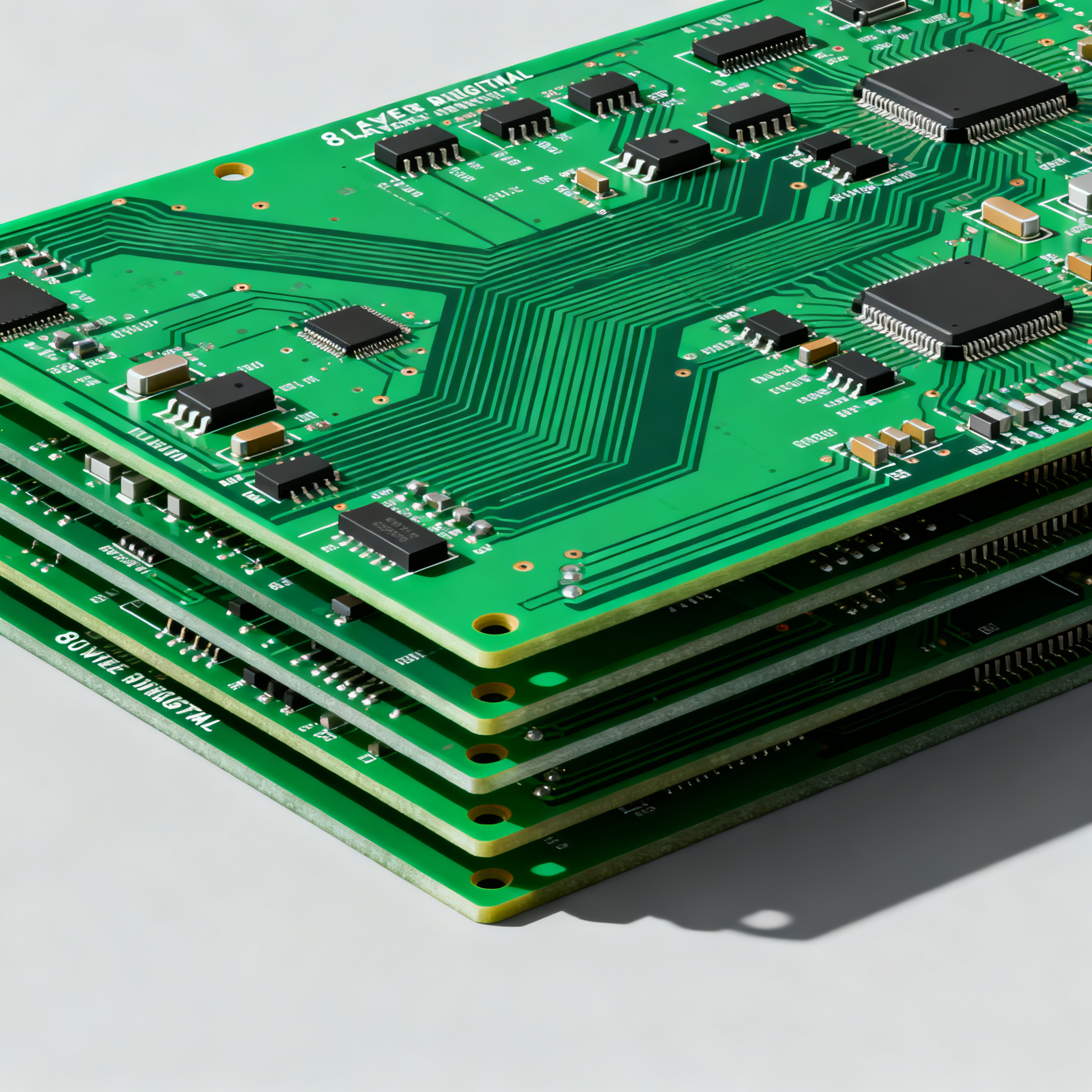
How to Achieve Best PCB Assembly Results: A Step-by-Step DFM Tutorial for 8-Layer Mixed-Signal Boards
Why 8-Layer Mixed-Signal Boards Fail at Assembly — and How DFM Prevents It An 8-layer mixed-signal board lives in a world of squeezed tolerances. Low‑noise analog front‑ends sit millimeters away from ...
Why 8-Layer Mixed-Signal Boards Fail at Assembly — and How DFM Prevents It
An 8-layer mixed-signal board lives in a world of squeezed tolerances. Low‑noise analog front‑ends sit millimeters away from fast DDR buses and switching regulators. The assembly line doesn’t see the elegant separation on your schematic — it sees a dense, thermally uneven composite that must survive lead‑free reflow without warping, tombstoning, or opening a single BGA ball. When a board bows just 0.3% across its diagonal, the stencil loses its seal, paste printing becomes erratic, and fine‑pitch components fail after reflow — not during functional test. This is the reality that NextPCB’s assembly guide captures: a warped board fails to form a proper seal with the solder paste stencil, causing printing defects, and can lift BGA balls off their pads, resulting in poor solder joints and costly rework.
Add to that the mix of analog and digital domains. A single overlooked return‑path discontinuity can couple digital transients into the analog reference plane, causing noise that survives reflow and appears as erratic ADC readings — a defect that no amount of post‑assembly tuning can fix. The root cause isn’t the soldering; it’s the stack‑up and copper balance. DFM (Design for Manufacturability) applied early and rigorously turns these hidden failure modes into controlled process steps. Instead of fighting yield loss at the reflow oven, you’re shipping boards that perform right out of the box.
This tutorial walks you through the DFM essentials specifically for 8‑layer mixed‑signal PCBs. We’ll anchor each step in real assembly physics and fabricator capability data, drawing on industry‑recognized DFM guidelines from 7pcb, component‑selection realities from Aimtron, and layout‑to‑yield relationships from Topfastpcb. By the end, you’ll have a concrete checklist and the confidence to get first‑pass assembly success.
The Stack-Up and Signal Integrity Foundation for Flawless Assembly
Before you route a single trace, the 8‑layer stack‑up is making promises to every signal on the board. It dictates impedance control, return‑path continuity, and — critically — the mechanical stability of the panel during reflow. A stack‑up that ignores factory capabilities or copper symmetry will bend, twist, and delaminate, no matter how clean the layout. The 7pcb rigid DFM guide reminds us that if the requirements of the PCB do not conform to the capacity of the factory — layer count, board thickness, surface finish — cost and lead time will be affected. But more than cost, a stack‑up that pushes a fabricator beyond its registered tolerances introduces impedance variance and layer‑to‑layer misregistration that can ruin mixed‑signal isolation.
A properly engineered stack‑up does more than hit a target impedance. It suppresses electromagnetic interference (EMI) and cross‑talk by providing solid, contiguous reference planes and tightly coupled routing layers. NextPCB’s design guide emphasizes that a well‑engineered stack‑up effectively addresses EMI, signal crosstalk, and impedance mismatch — issues that, if left unchecked, produce intermittent analog failures after assembly. For an 8‑layer board, we typically aim for a symmetric buildup with a central core, balanced prepreg layers, and a copper distribution that keeps the board flat through the 245–250°C peak of lead‑free reflow.
Tip: Always ask your fabricator for their preferred stack‑up table for 8‑layer designs with your target thickness (commonly 1.6 mm or 2.0 mm). They will provide the exact laminate types, copper weights, and pressed thicknesses that their process can reliably deliver. Start from that table, then adjust your impedance calculator, not the other way around.
Recommended 8‑Layer Stack‑Up Parameters for Mixed‑Signal Assembly
| Parameter | Typical Value / Range | Notes |
|---|---|---|
| Total board thickness | 1.6 mm ± 10% | Standard for assembly fixtures; 2.0 mm acceptable for high rigidity |
| Layer count | 8 | Signal, ground, power planes |
| Copper weight (outer layers) | 1 oz (35 µm) | Heavier copper (2 oz) increases warpage risk; use only if needed |
| Copper weight (inner layers) | 0.5 oz (18 µm) or 1 oz | Thinner copper aids fine‑line etching; keep symmetrical |
| Dielectric material | FR‑4, Tg ≥ 170°C | High‑Tg resists reflow warpage; mid‑loss materials for >5 GHz |
| Impedance tolerance | ±10% (single‑ended), ±7% (differential) | Tighter tolerances require tighter process control; confirm with fab |
| Core/prepreg thickness symmetry | Mirrored about center | E.g., core 0.2 mm top, core 0.2 mm bottom; identical prepreg stacks |
| Copper balance (layer pairs) | ≤ 10% difference in copper area | Use dummy copper fills on sparse layers to match heavy pours |
A symmetric copper balance is the single most effective way to prevent warpage. When one layer is heavily poured and its mirror image is sparse, the board bows during reflow, breaking the stencil seal and lifting BGA balls — exactly the failure described in the NextPCB assembly guide. The fix is to run a copper balance check once the layout is 90% complete. If plane layers are well‑filled but signal layers are not, add grounded dummy fills on those signal layers. The result is a board that stays flat, prints reliably, and solders without opens.
Equally important is the return‑path integrity for mixed‑signal domains. High‑speed digital signals must have an uninterrupted reference plane directly adjacent. If a digital trace crosses a split in the ground plane, the return current detours, creating a loop that radiates into the analog section. The stack‑up should therefore place the sensitive analog reference plane (usually a clean ground) on a dedicated inner layer, with the digital ground plane on another, and stitch them at a single point with filtering. This is a DFM concern because split planes require careful capacitor placement and can affect the etch uniformity of adjacent layers if not communicated to the fabricator.
Comparing 8-Layer Stack-Up Configurations: Stripline vs. Microstrip for Mixed-Signal Yields
Once the layer count is fixed, you face a critical choice: route critical signals on outer microstrip layers or bury them inside as stripline. Each configuration influences signal integrity, isolation, and the assembly tolerance budget. The Topfastpcb DFM guide notes that the layout quality of SMT components directly impacts assembly yield, and the choice of routing topology changes how those components are placed and how the stencil interacts with the board. At the same time, component availability and package selection — stressed by Aimtron’s DFM essentials — can dictate whether you can even use a tightly packed microstrip floorplan.
Below is a side‑by‑side comparison of the two primary 8‑layer mixed‑signal configurations. We’ll evaluate them on assembly flatness, isolation, routing density, and cost.
| Comparison Metric | Option A: Outer Microstrip (Top/Bottom Signal) | Option B: Buried Stripline (Inner Signal Layers) | Selection Criteria & Failure Boundary |
|---|---|---|---|
| Signal speed / edge rate | Faster propagation; lower dielectric loss (air above) | Slightly slower; fully surrounded by dielectric | Use microstrip for DDR/DDR4 interfaces; stripline for clocks where timing margin is critical |
| EMI / crosstalk isolation | Higher radiation; outer layers couple to external noise | Excellent shielding; signals buried between planes | Stripline preferred for analog front‑ends and sensitive ADC inputs to avoid digital noise coupling |
| Assembly flatness (warpage risk) | Exposed to asymmetric thermal expansion if outer copper is unbalanced | Inner layers less affected; but unbalanced inner copper can still warp | Both require copper balance; microstrip can be more sensitive to uneven outer copper, causing stencil seal loss |
| Impedance control tolerance | Impedance strongly affected by solder mask thickness and plating | Predictable impedance due to uniform dielectric thickness | Stripline yields tighter impedance tolerance (±7%) across the batch, reducing assembly‑related signal integrity failures |
| Routing density & BGA breakout | Easier to route; fewer vias needed for BGA escape | Requires more vias; can increase layer count and via aspect ratio | Microstrip helps with dense 0.8‑mm pitch BGAs; stripline may force blind vias, raising cost and yield risk |
For a mixed‑signal 8‑layer board, a hybrid approach often wins: keep the high‑speed digital busses on outer microstrip layers for routing ease, while burying the analog reference and low‑level sensor signals on inner stripline layers sandwiched between ground planes. This strategy isolates the sensitive analog nodes from digital noise while preserving the board’s ability to stay flat during reflow. However, the outer microstrip layers must still be balanced with dummy copper to match the inner plane fills. The component placement planning must also account for the stencil’s ability to print paste on fine‑pitch microstrip pads without solder bridging — a detail directly tied to the SMT layout quality referenced by Topfastpcb.
Before finalizing the stack‑up, confirm with your assembly partner that their equipment can handle the stencil thickness you’ll need. A mixed‑signal board often requires a 5‑mil (0.127 mm) stencil for 0.5‑mm pitch QFPs and 0201 discretes, while also demanding a 6‑mil stencil for larger BGA apertures. A stepped stencil or a dual‑thickness stencil can be a worthwhile investment for first‑pass yield.
A Step-by-Step DFM Walkthrough for Your 8-Layer Mixed-Signal Design
This section is the hands‑on sequence that takes your design from component selection to Gerber freeze. At each step, we’ll apply DFM thinking that is specific to an 8‑layer mixed‑signal board. The goal is not a generic checklist; it’s a series of decisions that directly prevent the assembly defects we’ve described.
- Component selection with assembly in mind. Begin by scrubbing your BOM for obsolete, non‑stocked, or single‑source parts. Aimtron’s DFM essentials stress that choosing readily available, standardized components compatible with your assembly equipment can significantly reduce lead times and prevent costly redesigns. For mixed‑signal boards, avoid legacy analog parts with unusual lead pitches or finishes that require special solder profiles. Prefer packages with exposed pads (e.g., QFN) that are designed for automated optical inspection (AOI).
- Symmetric stack‑up and copper balance. With your fabricator’s approved stack‑up in hand, assign layers: typically, Layers 1 and 8 are signal, 2 and 7 are ground planes, 3 and 6 are inner signal (stripline), 4 and 5 are power and ground (or split planes). Ensure that every layer’s copper pour has a mirror with equal copper area. FS PCBA’s DFM guidelines point out that imbalance in copper leads to bow and twist, which is a deal‑breaker for assembly. Use your CAD tool’s copper area calculation to verify that the difference between Layers 1 and 8, 2 and 7, etc., is less than 10%.
- Plane splits and stitching capacitor placement. If you must split the analog and digital ground on an inner plane, define the split line clearly and place stitching capacitors (typically 0.1 µF and 1 nF in parallel) across the gap where signals cross. This is not just a signal integrity detail; it affects assembly because the split creates an uneven copper distribution that can cause localized warping. Communicate the split’s location to the fabricator so they can adjust etching compensation.
- Trace width and spacing for etch tolerance. For high‑speed digital traces, calculate the required width and spacing based on the fabricator’s minimum etch tolerance. An 8‑layer board often uses 4‑mil (0.1 mm) traces and spaces on inner layers. If your BGA breakout forces a 3‑mil trace, confirm that the factory’s capability is 3/3 mil (trace/space) and that the impedance will still be within spec. The Sierra Circuits DFM rules remind us that drilling is the first manufacturing step, but etch precision directly impacts the solder mask dam between pads. Breakout traces that leave no room for a solder mask dam invite shorts during assembly.
- Paste mask design for fine‑pitch and BGA. The stencil aperture for a 0.4‑mm pitch BGA pad is typically 0.25 mm square, reduced from the 0.3 mm pad size. For 0.5‑mm pitch QFPs, a 0.2 mm‑wide aperture with a 0.15 mm length reduction is common. These dimensions must be documented in the paste mask layer. If you are using a via‑in‑pad under a BGA, the via must be plated over and capped (VIPPO) to prevent solder wicking. Review the paste mask openings with your assembly house before freezing the Gerbers; they can recommend a stepped stencil if needed.
- Copper pour and thermal relief design. On power and ground layers, use thermal relief spokes for through‑hole connectors and heavy copper pads. Without thermal reliefs, the large copper plane acts as a heat sink, causing cold solder joints during reflow. For surface‑mount pads connected to planes, a direct connection is acceptable for small components, but large passive pads (e.g., 1206) should use thermal ties to avoid tombstoning.
- Complete fabrication file package. Before sending the design to your assembler, compile the file set: Gerber files (all layers, including paste mask, solder mask, silkscreen, and board outline), IPC‑356 netlist, pick‑and‑place centroid data (ASCII format), a complete BOM with manufacturer part numbers and package descriptions, and a detailed fabrication drawing. The drawing must specify the stack‑up, impedance targets, board finish (ENIG recommended for mixed‑signal flatness), and any special requirements like VIPPO. Sierra Circuits’ DFM rules are clear: check whether all the files required for manufacturing are provided. Missing the IPC‑356 netlist, for example, blocks the automated DFM check that compares Gerber connectivity to the schematic.
- Involve the assembly partner early. Once the layout is 80% complete, share the provisional files with your assembly house. They can run a DFM review that flags issues like acid traps, insufficient annular rings, and stencil‑to‑pad mismatches. This is the point where you adjust stencil thickness, solder mask expansion, and panelization before the final freeze. At NovaPCBA, an early DFM review often catches copper balance issues and paste mask anomalies that would otherwise delay prototypes by weeks.
Pre‑Release DFM Checklist for 8‑Layer Mixed‑Signal Designs
| Checkpoint | Acceptable Criterion | Verification Method |
|---|---|---|
| Copper balance (layer pairs) | ≤ 10% difference in copper area | CAD copper area report; visual inspection of dummy fills |
| Stack‑up symmetry | Mirrored core & prepreg thicknesses | Fabricator’s stack‑up table; cross‑section measurements |
| Trace/space (inner layers) | ≥ 4/4 mil (typical); 3/3 mil if fab‑confirmed | DRC; fabricator capability confirmation |
| Solder mask dam width | ≥ 0.1 mm (4 mil) between pads | Gerber review; CAM tool check |
| Paste mask aperture reduction | BGA: 80–90% of pad area; QFP: 10–15% length reduction | Gerber overlay; stencil supplier DFM |
| Via‑in‑pad under BGA | Plated over and capped (VIPPO) | Fabrication drawing note; IPC‑4761 type VII |
| Plane splits & stitching caps | Split line defined; caps placed with short traces | Schematic review; placement check |
| File package completeness | Gerbers, IPC‑356, centroid, BOM, fab drawing | Checklist before upload |
This checklist is not exhaustive, but it targets the specific failure mechanisms of mixed‑signal 8‑layer boards. Run through it with your layout engineer and assembly partner. The investment of a few hours in DFM review saves weeks of debugging assemblies that fail inexplicably in the field.
Questions Engineers Ask Before Releasing 8-Layer Mixed-Signal Boards to Production
Q: What is the single biggest assembly risk when mixing low-noise analog and high-speed digital on an 8-layer board?
Return path discontinuity. Digital transients can couple into the analog reference plane if the stack‑up isn’t symmetric and the split planes aren’t handled with a careful stitching capacitor strategy. This noise survives reflow and appears as erratic ADC readings, not a visible solder defect. The fix is a DFM review that treats plane splits as assembly‑critical features, ensuring they are communicated to the fabricator and that stitching caps are placed directly over the split with minimal loop area.
Q: How do I prevent my 8-layer board from warping during lead-free reflow?
Enforce a symmetric layer stack‑up with equal copper distribution on mirrored layers. A balanced buildup prevents the uneven thermal expansion that warps boards, breaking stencil contact and lifting BGA balls [1]. Also keep core thicknesses symmetrical and avoid heavy copper on one side only. During layout, fill sparse signal layers with grounded copper pours to match the density of adjacent plane layers. If your board still bows, consider a high‑Tg laminate (Tg ≥ 170°C) and a thicker board (2.0 mm) for added rigidity.
Q: Is it worth using blind or buried vias in an 8-layer mixed-signal design, or should I stick to through-holes?
Blind/buried vias can solve routing density nightmares and shorten signal paths, but they add drilling cycles and cost, and their aspect ratio must match the factory’s capability [2]. For mixed‑signal, through‑holes with proper anti‑pad sizing often suffice if the floorplan is disciplined. Only commit to blind/buried vias when you need to isolate analog and digital returns on inner layers without breaking the bus. For example, a high‑density ADC with a 0.5‑mm pitch BGA may force blind vias to escape, but then you must also ensure the laser‑drilled via diameter is large enough for reliable plating — typically 0.1 mm minimum in a 0.2 mm pad.
Q: What exactly should I include in the design file package to get a useful DFM check from my assembler?
Provide Gerber files (all layers), IPC‑356 netlist, pick‑and‑place centroid data, a complete BOM with manufacturer part numbers, and a detailed fabrication drawing that specifies stack‑up, impedance targets, and board finish. Missing any of these files blocks the DFM analysis [5]. Also include a paste mask layer that matches your stencil intentions. The IPC‑356 netlist is crucial because it enables the assembler to compare the Gerber connectivity against the schematic, catching opens or shorts that a visual inspection would miss.
Q: How do I verify that a dense BGA breakout on an 8-layer board won't cause assembly opens or shorts?
Check breakout trace width and spacing against the fabricator’s etch tolerance, and ensure via‑in‑pad is plated over and capped if used. Then simulate the paste deposit: the stencil aperture for BGA pads must be smaller than the pad size but large enough to print a reliable brick. Assembly yield often drops when the breakout leaves no room for a proper solder mask dam between pads. A minimum 0.1 mm solder mask dam is required to prevent bridging. If your layout forces a smaller dam, consider a solder mask defined (SMD) pad or a non‑solder mask defined (NSMD) pad with a wider clearance, but always consult your assembler.
Q: What is the DFM deal-breaker that most often delays 8-layer mixed-signal prototypes, and how can I avoid it?
Unbalanced copper. When one layer is heavily poured and its mirror is sparse, the board bows and the stencil can’t seal [6]. This is caught late because electrical simulation doesn’t flag it. Run a copper balance check before freezing the layout, and add dummy fills on signal layers if needed. The dummy fills should be grounded to avoid floating metal that can radiate. A simple rule: every signal layer must have a copper pour, even if it’s not a dedicated plane, and the pour area must be within 10% of its opposite layer.
References & Further Reading
- PCB Assembly Design Guide: DFM, DFA, and Best Practices for 2026 – NextPCB
- Rigid PCB Design For Manufacturability Guide – 7pcb (Updated Feb 2025)
- Complete Guide to PCB Design for Manufacturability (DFM) – Topfastpcb
- Design It Right, Build It Better: DFM Essentials for PCB Assembly – Aimtron
- DFM Rules – Sierra Circuits
- PCB DFM (Design for Manufacturing) Guidelines and Checklists – FS PCBA
Need a partner who understands the assembly challenges of mixed‑signal 8‑layer boards? At NovaPCBA, we bring together advanced DFM analysis, high‑precision SMT lines, and a fabrication network that can handle your tightest impedance and via requirements. Our team reviews every 8‑layer design for copper balance, stack‑up symmetry, and paste mask integrity before the first prototype is built. Contact NovaPCBA today to discuss your next mixed‑signal project and get a free DFM consultation.