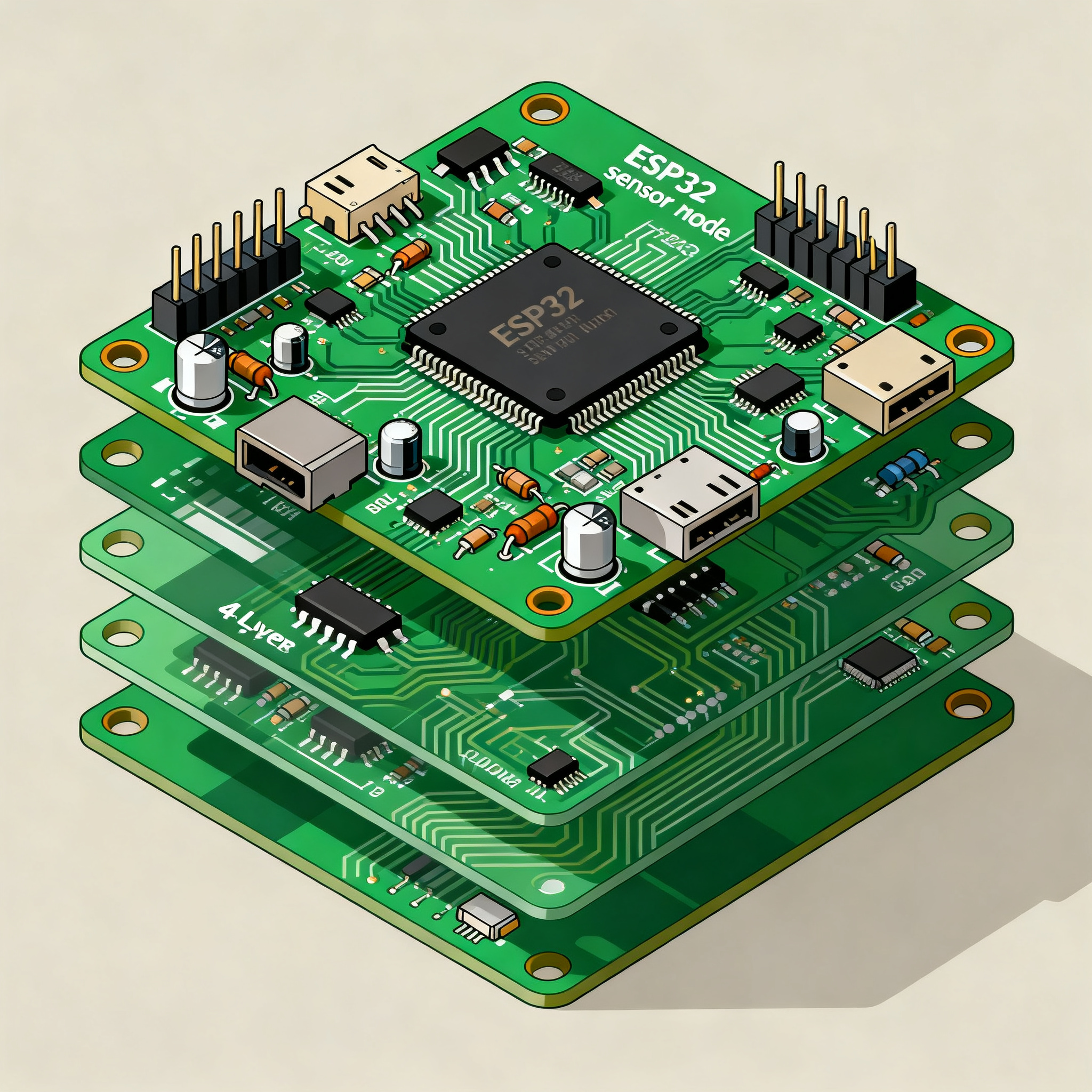
How PCBasic’s IoT PCB Assembly Powers Smart Connectivity: A 4-Layer ESP32-Based Sensor Node Case Study
How PCBasic's IoT PCB Assembly Powers Smart Connectivity: A 4-Layer ESP32-Based Sensor Node Case Study When One Defect Can Brick a Sensor Node: Why IoT PCB Assembly Reliability Matters Now Picture thi...
When One Defect Can Brick a Sensor Node: Why IoT PCB Assembly Reliability Matters Now
Picture this: a fleet of 2,000 wireless environmental sensor nodes deployed across a pharmaceutical cold-chain warehouse. Each node runs an ESP32 module, sampling temperature and humidity every 30 seconds and pushing data to a cloud dashboard via Wi-Fi. Six months in, 47 nodes go dark. The root cause? A single tombstoned 0402 capacitor on the RF matching network—barely visible under a microscope—that drifted into an open circuit after thermal cycling. The recall costs, field-replacement labor, and compliance paperwork ran well into six figures. And the culprit was not a design flaw; it was an assembly defect that slipped through a supplier's inspection process.
This scenario is not hypothetical. As AllPCB's IoT assembly best-practices analysis bluntly states, "even a single defect can render a device unusable, leading to costly recalls or customer dissatisfaction." In the IoT space—where sensor nodes are expected to operate unattended for years on battery power, often in harsh environments—the margin for assembly error shrinks to near zero. A cold solder joint on a QFN package, a micro-void in a BGA ball, or insufficient solder paste on a fine-pitch connector can all produce intermittent failures that are maddeningly difficult to reproduce on a bench.
The stakes are climbing. Smart home devices, industrial predictive-maintenance sensors, and agricultural IoT nodes all share a common DNA: they integrate wireless communication modules (Wi-Fi, Bluetooth, Zigbee), low-power microcontrollers, analog front-ends, and power-management circuits onto compact PCBs. PCBasic's IoT PCB assembly overview notes that these devices "usually integrate wireless communication modules such as Wi-Fi, Bluetooth, and Zigbee, and require low-power, stable IoT PCB solutions." The phrase "stable" does the heavy lifting here—it is not about whether the board works on the lab bench; it is about whether it still works after 500 thermal cycles in a non-climate-controlled enclosure.
PCBasic's PCB failure analysis insights reinforce this point: many field failures trace back not to component defects but to process weaknesses during assembly—poor wetting, insufficient reflow profiling, or contamination under components. When you combine these risks with the pressures of accelerating time-to-market, the case for a reliability-first assembly partner becomes compelling. Pcbandassembly's IoT assembly page captures the requirement succinctly: IoT PCB assembly must be "built for connectivity, low-power operation, and long-term reliability." That triad—connectivity, low power, longevity—defines the lens through which every solder joint, every via, and every inspection step must be evaluated.
Key Takeaway: In IoT sensor nodes, a single assembly defect is not a quality statistic—it is a business risk. The cost of catching that defect at AOI is measured in cents; the cost of catching it in the field is measured in thousands of dollars per node, plus reputational damage. PCBasic's turnkey IoT PCB assembly approach addresses this by layering inspection at every stage—SPI, AOI, ICT, and functional test—so that the 47 dark nodes in the warehouse never happen.
Inside the 4-Layer Stack-Up That Keeps an ESP32 Sensor Node Connected
The ESP32 is a marvel of integration: dual-core Xtensa processor, Wi-Fi 802.11 b/g/n, Bluetooth 4.2/BLE, and a respectable set of peripherals—all in a single QFN package. But that integration comes with a price: the RF section demands controlled impedance, the digital core generates fast edge rates, and the power amplifier can pull current spikes that would make a poorly designed power distribution network (PDN) sag. This is where the PCB stack-up stops being an afterthought and becomes a critical design element.
A 4-layer board following the signal–ground–power–signal (S-G-P-S) arrangement gives the ESP32 exactly what it needs. Layer 1 (top) carries the RF traces, the antenna matching network, and the high-speed digital buses. Layer 2 is a continuous ground plane that provides an unimpeded return path for every signal on Layer 1—this is non-negotiable for controlled impedance and EMI containment. Layer 3 is a power plane, often split into multiple voltage rails (3.3V for the ESP32, 1.8V for sensors, and possibly a boosted rail for analog). Layer 4 (bottom) handles low-speed signals, I²C, SPI, and the programming header.
PCBasic's 4-layer PCB design guide provides the foundational parameters that make this stack-up work. The standard 1.6 mm total thickness is a good starting point, but for IoT nodes in compact enclosures, 1.0 mm or even 0.8 mm options are available. Below is a representative stack-up table for an ESP32-based sensor node, drawn from PCBasic's manufacturing capabilities and typical IoT design requirements.
| Parameter | Typical Value | Unit / Notes |
|---|---|---|
| Total board thickness | 1.6 (standard); 0.8–3.2 available | mm |
| Layer count | 4 | Signal / GND / Power / Signal |
| Core material | FR-4, Tg 130–150°C | Standard; high-Tg available for lead-free |
| Core thickness (L2–L3) | 0.6–1.0 | mm |
| Prepreg type (L1–L2, L3–L4) | 2116 or 7628 | Depends on impedance target |
| Copper weight (outer layers) | 1 oz (35 µm) | Standard; 0.5 oz for fine-pitch |
| Copper weight (inner layers) | 0.5 oz (17.5 µm) | Typical for planes |
| Impedance target (RF traces) | 50 Ω ±10% | Microstrip on L1, referenced to L2 GND |
| Minimum trace/space | 4/4 mil (0.1/0.1 mm) | Standard; 3/3 mil available |
| Minimum drill diameter | 0.2 | mm (mechanical) |
| Surface finish | ENIG (electroless nickel immersion gold) | Preferred for RF and fine-pitch |
| Solder mask | Green, LPI | Other colors available |
This stack-up is not just about layer count—it is about what each layer does for signal integrity. The continuous ground plane on Layer 2 means that every RF microstrip on Layer 1 has a well-defined, low-inductance return path directly beneath it. That is the difference between a 50 Ω trace that actually measures 50 Ω across the 2.4 GHz ISM band and one that drifts to 65 Ω, causing impedance mismatch, reflected power, and reduced range. For a BLE sensor node that needs to punch through a few walls, that mismatch can mean the difference between reliable data delivery and dropped packets.
The SMT assembly side is equally nuanced. PCBSync's IoT PCB guide advises that "you'll want to push toward smaller packages (0402 or even 0201 passives) where your assembly process supports it." The ESP32 module itself is often a SiP (System-in-Package) with a fine-pitch QFN or LGA footprint. Placing these components requires precise solder paste deposition—typically through a laser-cut stainless steel stencil with 0.1 mm thickness for fine-pitch pads—and a reflow profile tuned to the thermal mass of the module. PCBasic's assembly line uses automated SMT pick-and-place machines with vision alignment capable of handling 0201 passives and 0.4 mm-pitch BGAs, backed by Solder Paste Inspection (SPI) to catch stencil printing defects before components are placed.
Tip: When specifying a 4-layer stack-up for an ESP32 design, ask your fabricator to provide a controlled-impedance coupon report. This is a small test coupon built on the same panel that verifies the actual impedance of representative traces. Without it, you are trusting the simulator—and simulation is only as good as the dielectric constant and prepreg thickness assumptions fed into it.
2 Layers Too Few, 6 Too Many? Comparing PCB Options for Wi-Fi IoT Devices
Every hardware engineer has faced the layer-count decision: do you try to squeeze the design onto a 2-layer board and save 15–20% on the bare PCB cost, or do you go to 4 layers and sleep better at night? For an ESP32-based sensor node with Wi-Fi and BLE, the answer is increasingly clear, but the trade-offs are worth examining in detail.
PCBSync's analysis puts it diplomatically: "For simple IoT devices with basic connectivity (like a Bluetooth sensor node), you might get away with 2 layers, though 4 is more comfortable." The key word is "comfortable." A 2-layer board forces the designer to route the RF section on the same layer as power distribution, with a fragmented ground plane stitched together by vias. The result is a ground return path that meanders around routed traces, creating loop inductance that degrades signal integrity and radiates EMI. For a BLE-only sensor node with a simple chip antenna, a carefully laid-out 2-layer board can work. Add Wi-Fi, an external flash chip, and a few sensors, and the routing becomes a game of Tetris where the penalty for losing is a non-functional RF front end.
Pcbandassembly's IoT PCB assembly guide states the consensus: "For Wi-Fi devices or anything with significant digital complexity, 4–6 layers is typical." Six layers enter the picture when you need additional routing space for high-density interconnects, multiple voltage domains, or sensitive analog sections that require shielding. But for the majority of ESP32 sensor nodes, 6 layers add cost without adding capability—the extra two layers might sit largely unpopulated, increasing the BOM and lengthening the fabrication cycle without any measurable improvement in RF performance.
The table below compares the three realistic options for an ESP32 sensor node, factoring in not just PCB cost but the downstream impacts on assembly yield, testability, and field reliability.
| Comparison Metric | 2-Layer PCB | 4-Layer PCB (PCBasic Recommended) | 6-Layer PCB | Selection Criteria & Failure Boundary |
|---|---|---|---|---|
| Signal integrity (RF) | Poor—fragmented ground, no controlled impedance plane | Good—solid GND plane on L2, 50 Ω microstrip achievable | Excellent—additional routing layers for isolation | 2-layer fails for Wi-Fi above 2.4 GHz; 6-layer is overkill unless multiple RF paths exist |
| BOM cost (bare PCB) | $0.30–0.60 per sq. in. (low volume) | $0.80–1.50 per sq. in. (low volume) | $1.50–3.00 per sq. in. (low volume) | 4-layer adds ~$1–2 per board at prototype volumes; 6-layer doubles that premium |
| Routing density | Low—all signals on two layers, ground fills compete with traces | Moderate—two signal layers plus dedicated planes | High—four signal layers available | 2-layer becomes unrouteable past ~60% component density on a 50×50 mm board |
| EMI performance | Marginal—large loop areas, no continuous return path | Good—tight coupling between signal and GND plane minimizes radiation | Very good—additional ground layers can sandwich high-speed signals | 2-layer risks FCC/CE radiated emissions failure; 4-layer passes with reasonable layout |
| Power integrity | Poor—PDN relies on wide traces, high IR drop | Good—dedicated power plane reduces IR drop and inductance | Excellent—multiple power planes can be dedicated to different rails | ESP32 transmit current spikes (~500 mA) cause voltage sag on 2-layer boards without careful decoupling |
| Assembly yield | Lower—warpage risk on thin 2-layer boards; no plane for thermal relief | High—balanced stack-up resists warpage; planes aid thermal distribution during reflow | High—but more layers mean more vias, increasing drill defects | 4-layer hits the sweet spot for reflow uniformity and minimal warpage |
| Design cycle time | Longer—more time spent on layout workarounds | Shorter—clean layer discipline reduces layout iterations | Longer—more layers to manage, more complex DFM | 4-layer saves 1–2 weeks of layout time vs. fighting a 2-layer board |
What the table does not capture is the assembly partner's role in making the 4-layer choice work. Programming Insider's top-5 IoT PCB assembly manufacturer list emphasizes that "buyers should check whether the supplier can manage small pads, fine-pitch ICs, module placement, ESD-sensitive parts, and mixed component types. SPI and AOI are important for solder paste and placement." This is where PCBasic differentiates from generic assemblers who may only offer basic SMT lines without the inspection infrastructure to catch the defects that a 4-layer RF board is susceptible to. Tombstoning on 0402 passives, bridging on 0.5 mm-pitch QFN pads, and voiding under the ESP32 module's thermal pad are all real risks that AOI and X-ray inspection can catch—if the assembler has the equipment and the engineering discipline to use it.
Key Takeaway: The 2-layer vs. 4-layer decision is not a cost decision—it is a reliability decision. A 2-layer board that passes bench testing but fails in the field after 100 thermal cycles costs far more than the $1.50 saved on the bare PCB. PCBasic's 4-layer ESP32 sensor node approach acknowledges that Wi-Fi connectivity demands a solid ground plane, and that the incremental cost of two additional layers is the cheapest insurance policy you can buy for an IoT product.
From Schematic to Shipment: A Practical Guide to Specifying and Sourcing PCBasic IoT PCB Assembly
You have the schematic, the layout is done, and the BOM is locked. Now comes the step that separates a smooth production ramp from a six-month debugging nightmare: specifying and sourcing the PCB assembly. The following guide walks through the practical decisions that matter for an ESP32-based sensor node, with actionable steps for engineers and procurement leads.
Step 1: Define Your Stack-Up and Material Requirements
Before sending Gerber files, document the stack-up explicitly. Specify the layer sequence (S-G-P-S), the dielectric thickness between L1 and L2 (this determines your 50 Ω trace width), the copper weight on each layer, and the surface finish. For an ESP32 design, ENIG is the preferred surface finish—it provides a flat, solderable surface for fine-pitch QFN pads and does not oxidize like HASL. Pcbandassembly's material advice notes that "for many IoT projects, standard FR-4 works fine. But if your device needs to bend, survive extreme heat, or fit into unusual shapes, polyimide is worth the additional cost." For most indoor sensor nodes, high-Tg FR-4 (Tg ≥ 150°C) is sufficient to survive multiple reflow cycles and operational temperature swings.
Step 2: Enforce DFM Rules for Antenna Keep-Out Zones
The ESP32 module's PCB trace antenna or external chip antenna demands a strict keep-out zone. This means no copper pour, no ground planes, and no components within the antenna's near-field region—typically a rectangular area extending 10–15 mm from the antenna element, on all layers. PCBSync's IoT PCB design guide emphasizes that multilayer PCBs "let you route signals on internal layers, freeing up surface area for components." Use that freedom wisely: route digital signals away from the antenna keep-out zone on internal layers, and place the module near the board edge with the antenna facing outward. PCBasic's DFM review checks for antenna clearance violations, ensuring that your carefully simulated antenna pattern is not detuned by nearby copper.
Step 3: Choose the Right Surface Finish and Solder Mask
ENIG is the default choice for RF boards, but it is worth understanding why. HASL (hot air solder leveling) leaves a slightly uneven surface that can cause coplanarity issues for QFN and LGA packages. The ESP32 module's thermal pad needs a flat, consistent surface for reliable soldering—ENIG delivers that. If cost is a concern and the design uses only larger-pitch components, lead-free HASL may be acceptable, but the trade-off in assembly yield for fine-pitch parts usually negates the cost savings.
Step 4: Specify Inspection and Test Protocols
AllPCB's quality control guidance identifies automated optical inspection as "a powerful tool to catch issues early." But AOI alone is not enough for a multi-step assembly process. The sequence that PCBasic applies to IoT assemblies includes:
- Solder Paste Inspection (SPI): 3D measurement of solder paste volume, area, and height on every pad before component placement. Catches insufficient paste, bridging, and misaligned stencils.
- Automated Optical Inspection (AOI): Post-reflow visual inspection of every solder joint, checking for tombstoning, bridging, insufficient solder, and component misalignment.
- In-Circuit Testing (ICT): Flying-probe or fixture-based electrical testing that verifies continuity, shorts, and passive component values on the assembled board.
- Functional Testing: Application-specific testing that powers up the board, verifies the ESP32 boots, checks RF output power, and reads sensor data. This is the test that catches what AOI and ICT miss—a board that is electrically correct but functionally dead.
- Burn-In (optional): For high-reliability applications, extended powered operation at elevated temperature to weed out infant mortality failures.
Step 5: Communicate Component Sourcing Strategy
Tell your assembler which components are critical, which have long lead times, and which have acceptable alternatives. PCBasic's turnkey IoT assembly service includes component procurement with access to franchised distributors and verified supply chains. In the current semiconductor environment, Espressif modules can have fluctuating lead times—PCBasic's procurement team can source compatible modules or recommend pin-compatible alternatives when the primary part is unavailable. This is not just about availability; it is about avoiding counterfeit parts, which are a growing problem for popular IoT ICs.
| Process Step | What to Specify | Why It Matters for ESP32 Sensor Nodes | PCBasic Capability |
|---|---|---|---|
| Stencil design | Thickness: 0.1 mm for fine-pitch; step-down for thermal pad | Prevents solder bridging on 0.5 mm-pitch QFN pads | Laser-cut stainless steel, electro-polished |
| Reflow profile | Peak temp 235–245°C (lead-free); soak zone 150–180°C for 60–90 sec | Avoids thermal shock to ESP32 module; ensures proper wetting | 10-zone reflow ovens with profile verification |
| ESD protection | Ionizers, grounded workstations, ESD-safe packaging | ESP32 RF inputs are sensitive to ESD damage; latent failures appear weeks later | Full ESD-protected production line |
| Conformal coating | Acrylic or silicone; mask connectors and antenna areas | Protects against humidity and condensation in outdoor or industrial sensor nodes | Selective coating application available |
| Testing | AOI + ICT + functional (RF power check, sensor readout) | Catches assembly defects that would cause field failures in always-on IoT nodes | Full inspection chain: SPI → AOI → ICT → Functional |
Note: When requesting a turnkey assembly quote, include the following in your RFQ: Gerber files (RS-274X or ODB++), BOM with manufacturer part numbers, pick-and-place file (centroid data), assembly drawing showing component locations and orientation, and any special instructions for antenna keep-out zones, conformal coating, or testing requirements. The more complete your documentation, the faster and more accurate the quote will be.
Your IoT PCB Assembly Questions, Answered by Engineers Who Build Sensor Nodes
After shipping hundreds of ESP32-based IoT designs, certain questions come up repeatedly. Here are the five that senior hardware engineers and procurement leads ask most often—with answers grounded in the realities of manufacturing, not textbook theory.
Q: Why did PCBasic's ESP32 sensor node design use a 4-layer stack-up instead of a cheaper 2-layer board?
The ESP32's Wi-Fi/Bluetooth radio and high-speed digital buses—SPI flash running at 80 MHz, I²S audio, and the SDIO interface—require controlled impedance and a solid ground plane for EMI management. A 2-layer board would force the RF traces to share a layer with power distribution and digital routing, creating a fragmented ground return path that degrades signal integrity and increases radiated emissions. The 4-layer stack-up (signal/GND/power/signal) provides clean return paths directly beneath every RF trace, reducing crosstalk and ensuring the 50 Ω impedance target is met across the 2.4 GHz band. The cost premium is typically $1–2 per board at prototype volumes—a small price for a design that passes FCC compliance testing on the first attempt and delivers reliable connectivity in the field.
Q: What DFM checks does PCBasic apply to antenna keep-out areas and fine-pitch components?
PCBasic's engineering team performs a comprehensive DFM review before fabrication begins. For antenna keep-out areas, they verify that no copper pour, ground planes, or components encroach on the specified clearance zone around the PCB trace antenna or chip antenna—typically 10–15 mm on all layers. They also check pad geometries for 0.5 mm-pitch QFN packages (the ESP32's footprint) and 0402 passives, ensuring that the stencil aperture design provides adequate solder paste volume without risk of bridging. During assembly, Solder Paste Inspection (SPI) measures paste deposition on every pad before component placement, and Automated Optical Inspection (AOI) verifies post-reflow solder joint quality. These steps catch common defects like tombstoning on 0402 capacitors and bridging on fine-pitch ICs before the boards leave the production line.
Q: How does PCBasic handle component sourcing for Espressif modules and other IoT-specific ICs during supply crunches?
PCBasic offers turnkey procurement with access to a verified supply chain that includes franchised distributors (Digi-Key, Mouser, Arrow, Avnet) and direct relationships with manufacturers. When Espressif ESP32 module lead times extend—a recurring challenge in the semiconductor market—PCBasic's procurement team can source alternative compatible modules (such as pin-compatible variants from Espressif's own lineup or modules from other certified manufacturers) and perform incoming inspection to verify authenticity. This includes visual inspection, marking verification, and electrical testing of sample units. The goal is to keep your production line moving without introducing counterfeit components, which are a known risk for popular IoT ICs in secondary markets.
Q: What testing and inspection protocols does PCBasic use to guarantee reliability before shipping?
Beyond AOI and SPI, PCBasic performs flying-probe or fixture-based in-circuit testing (ICT) to verify continuity, isolation, and passive component values. For IoT sensor nodes, functional testing is tailored to the application: the board is powered up, the ESP32 module is programmed with a test firmware, and key parameters are verified—RF output power at the antenna port, sensor readout accuracy (e.g., temperature/humidity sensor values within tolerance), and communication link establishment with a test access point. For high-reliability applications such as industrial monitoring or medical cold-chain sensors, PCBasic can add burn-in testing (extended powered operation at elevated temperature) and conformal coating to protect against moisture and contaminants. All inspection and test results are documented against IPC-A-610 Class 2 or Class 3 acceptance criteria, depending on the application requirements.
Q: What is the typical lead time and minimum order quantity for a 4-layer IoT PCB assembly with PCBasic?
Standard lead times for a 4-layer turnkey assembly range from 5 to 15 working days, depending on complexity, component availability, and order volume. Prototype builds (1–20 pieces) typically ship in 5–8 working days if all components are in stock. Small-batch production runs (50–500 pieces) are generally 10–15 working days. PCBasic accepts prototypes from a single piece, small-batch runs, and scales to mass production, with no rigid minimum order quantity constraints. This flexibility is particularly valuable for IoT startups that need to iterate on their design with small prototype batches before committing to volume production. For orders where component lead times are a concern, PCBasic can provide a partial-build option: assemble the boards with in-stock components and ship them, then complete the assembly when the remaining components arrive.
References & Further Reading
- IoT PCB Assembly: Enabling Smart Connectivity with PCBasic — PCBasic's overview of turnkey IoT PCB assembly manufacturing, covering smart home, industrial, and low-power applications.
- IoT PCB Assembly: Driving the Future of Connected Devices — PCBasic's analysis of PCB failure modes in IoT devices and best practices for prevention.
- IoT PCB Assembly – Smart Connectivity Solutions — Pcbandassembly's guide to IoT PCB assembly, covering layer-count selection, materials, and reliability requirements.
- IoT PCB Assembly: Best Practices for Reliable and Efficient Manufacturing — AllPCB's quality control recommendations, emphasizing AOI and defect prevention.
- IoT PCB: Everything You Need to Know (Design, Materials & Best Practices) — PCBSync's comprehensive IoT PCB design guide covering stack-ups, SMT packaging, and SiP modules.
- 4-Layer PCBs: Stack-Up, Thickness, and Design Tips — PCBasic's technical reference for 4-layer PCB design parameters and cost optimization.
- Top 5 IoT and Smart Home PCB Assembly Manufacturers for Connected Devices — Programming Insider's evaluation criteria for selecting IoT PCB assembly partners.
- NovaPCBA — PCB Assembly Services — For additional turnkey PCB assembly capabilities, including IoT and RF designs, NovaPCBA offers complementary manufacturing solutions with fast-turn prototyping and volume production.