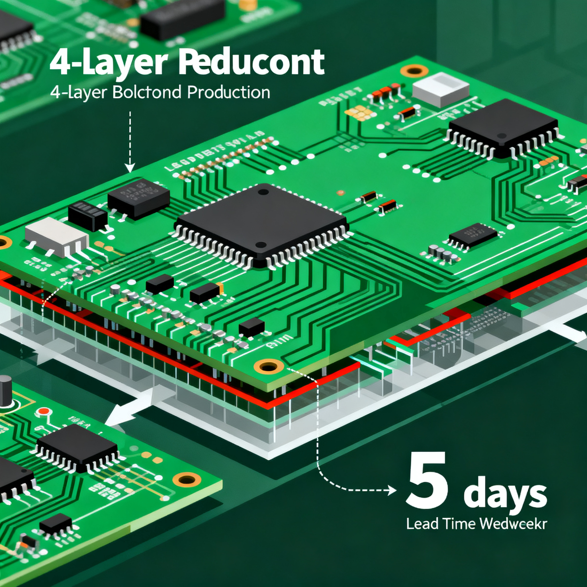
How 4-Layer PCB Production Lead Times Shrank from 3 Weeks to 5 Days: Real-World Examples
Why 3-Week 4-Layer Lead Times Forced a Manufacturing Reset Three weeks sounds manageable until you lose a product launch window by four days. That was the reality confronting engineering teams across ...
Why 3-Week 4-Layer Lead Times Forced a Manufacturing Reset
Three weeks sounds manageable until you lose a product launch window by four days. That was the reality confronting engineering teams across North America and Europe between 2021 and early 2024, when standard 4-layer PCB lead times stretched past 15 business days—and occasionally past 20—due to laminate shortages, copper foil allocation battles, and overwhelmed drilling capacity at mid-tier fabrication houses. For a hardware startup burning $80,000 a month in payroll waiting on prototype boards, or an automotive Tier-2 supplier facing liquidated damages of $1,200 per day for late validation samples, the math stopped working.
The pain wasn't evenly distributed. Large OEMs with six-figure annual PCB spends could negotiate priority slots. Small and mid-volume buyers—the ones driving most new product introductions—got squeezed. A 4-layer board that should have landed in 12 working days suddenly took 18, then 21, then slipped again without explanation. The project Gantt chart became fiction. Mechanical enclosures arrived before the PCB could be populated. Firmware engineers sat idle. Marketing teams delayed press embargoes. The ripple effects of a 3-week lead time touched every department, yet procurement had few levers to pull.
What changed wasn't a single breakthrough but a convergence of pressures. Fabricators who had invested in automated direct imaging (LDI) systems and laser direct imaging for solder mask found those capital expenditures suddenly paying off. CAM engineers, traditionally the bottleneck in front-end processing, saw their workflows compressed from 8-10 hours of manual stackup verification to under 90 minutes through intelligent automation and pre-approved stackup libraries aligned with IPC-2221 design standards. Panel utilization algorithms that once ran overnight now completed in minutes, optimizing multiple 4-layer jobs onto shared production panels without human intervention.
Equally important was a shift in buyer behavior. Engineering teams that had treated PCB fabrication as a commodity purchase—send Gerbers, wait three weeks, complain about delays—began treating it as a design-integrated process. They submitted clean ODB++ packages instead of flat Gerber archives. They pre-negotiated stackup approvals. They stopped specifying exotic materials where standard high-Tg FR-4 would suffice. This behavioral reset, combined with fabricator automation, created the conditions for 5-day 4-layer production to move from marketing claim to operational reality. The 3-week standard didn't fall gradually; it collapsed under the weight of its own opportunity cost.
Inside the 4-Layer Fabrication Pipeline: Why 3 Weeks Was Standard and How 5 Days Became Possible
To understand the magnitude of compressing 15+ working days into five, you need to walk the actual fabrication sequence. A standard 4-layer board isn't simply two double-sided cores glued together. Each step carries dwell time, queue time, and inspection gates that historically accumulated into a multi-week process. The table below contrasts the legacy timeline with what modern quick-turn lines achieve today.
| Process Step | Legacy 3-Week Cycle (Working Days) | Modern 5-Day Quick-Turn (Working Days) | Key Enabler |
|---|---|---|---|
| CAM engineering & stackup verification | 2.0–3.0 | 0.5–1.0 | Automated DRC/DFM with pre-approved stackup libraries per IPC-2221 |
| Material issuance & inner layer imaging | 2.0–2.5 | 0.5–1.0 | Laser direct imaging (LDI); no film generation required |
| Inner layer etching & AOI | 1.5–2.0 | 0.5 | Inline automated optical inspection with AI-based defect classification |
| Oxide treatment & layup | 1.0 | 0.5 | Pre-cut prepreg kits; automated layup stations |
| Lamination & cooling | 2.0–2.5 | 1.0 | Hot press optimization; reduced cool-down under controlled atmosphere |
| Drilling (through-hole + optional vias) | 1.5–2.0 | 0.5–1.0 | Multi-spindle drilling with shared panel pooling |
| Electroless copper & panel plating | 1.5–2.0 | 0.5 | Horizontal continuous plating lines; no batch tank dwell |
| Outer layer imaging & etching | 1.5–2.0 | 0.5–1.0 | LDI; merged inner/outer layer workflows |
| Solder mask & legend printing | 1.5–2.0 | 0.5 | LDI solder mask; UV-cure tack-dry in minutes |
| Surface finish (ENIG, HASL, or OSP) | 1.0–1.5 | 0.5 | Inline ENIG lines replacing batch immersion |
| Electrical test (flying probe or fixture) | 1.0–2.0 | 0.5 | High-speed flying probe; parallel test stations |
| Final inspection & shipping | 1.0 | 0.5 | Automated visual inspection per IPC-A-610 Class 2 criteria |
| Total working days | 15–22 | 4–6 | Parallel processing + automation + pre-approved data |
The numbers tell only part of the story. The real transformation happened in how work flows through the factory. Legacy fabrication treated each PCB order as a sequential serial job: one panel entered lamination, then waited for cooling, then queued for drilling. Modern quick-turn lines use parallel panel processing—splitting an order across multiple lamination presses and drill stations simultaneously, then re-merging panels at electrical test. This alone can cut three calendar days from a 4-layer build without touching per-step cycle time.
Another critical shift involved the elimination of film-based imaging. Traditional photolithography required generating physical photomasks for each layer—a step that consumed hours per artwork and introduced registration tolerance stack-ups. Direct imaging writes the pattern straight from digital CAM data onto the photoresist-coated panel. For a 4-layer board with solder mask, that eliminates four film-generation cycles and their associated handling, inspection, and storage. Combined with automated CAM systems that validate designs against IPC-A-610 inspection criteria before a single panel enters production, the front-end bottleneck largely disappeared.
Tip: If your current fabricator still quotes 12–15 working days for a standard 4-layer board with no special requirements, they are likely running a batch-oriented, film-based line. The technology gap between batch and continuous-flow fabrication now exceeds a full week of cycle time.
5 Days vs. 3 Weeks: Real Cost, Quality, and Design Restrictions for 4-Layer Stacks
Faster isn't always better, and cheaper isn't always cheaper. The table below maps the real trade-offs engineering and procurement teams encounter when choosing between accelerated and standard 4-layer production. These numbers reflect typical mid-volume pricing from established Asian and North American fabricators serving prototyping and bridge-tooling markets.
| Comparison Metric | 5-Day Quick-Turn 4-Layer | 3-Week Standard-Turn 4-Layer | Selection Criteria & Failure Boundary |
|---|---|---|---|
| Typical price adder vs. baseline | 50–100% above standard pricing | Baseline (reference price) | Justify premium when NPI schedule compression saves >2 days of engineer idle time |
| Minimum lot size | 5–30 panels (often 5-piece minimum) | No practical minimum; 1 panel viable | Below 5 panels, 5-day pricing becomes punitive; above 30 panels, pooled sharing loses efficiency |
| Material restrictions | Standard high-Tg FR-4 (170°C Tg), some mid-Tg options | Full range: FR-4, Rogers, Teflon, polyimide, mixed laminates | Choose standard when exotic dielectrics are non-negotiable; choose quick-turn for FR-4 designs |
| Controlled impedance | Available on limited stackup configurations; ±10% tolerance typical | Full impedance modeling; ±5–7% tolerance achievable | Quick-turn acceptable for digital buses (USB, HDMI); tighter tolerances need standard-turn for RF paths |
| Blind/buried vias | Generally not supported or adds 2–3 days | Fully supported; sequential lamination standard | Designs with blind/buried vias should default to standard-turn unless fab explicitly confirms quick-turn capability |
| Surface finish options | ENIG, HASL (lead-free), OSP | ENIG, ENEPIG, immersion silver, immersion tin, HASL, OSP, hard gold | Quick-turn covers 90% of commercial applications; ENEPIG or hard gold pushes to standard |
| Registration tolerance | ±3–4 mil typical | ±2–3 mil typical | Fine-pitch BGAs (0.5 mm pitch and below) benefit from standard-turn registration margins |
| Solder mask color options | Green, sometimes blue or black | Full palette available | Cosmetic requirements rarely justify standard-turn premium unless branding mandates specific color |
| Risk of respin due to process corners | Moderate—tighter process windows mean less margin for DFM issues | Lower—more time for CAM review and rework if needed | Submit only fully DFM-checked designs to quick-turn; save experimental layouts for standard-turn |
| Best-fit application | Prototype validation, bridge tooling, urgent NPI builds, trade show samples | Pre-production, cost-sensitive production, complex HDI stacks, qualification builds | Align lead time choice with project phase, not habit |
The table reveals a pattern that seasoned buyers recognize: quick-turn 4-layer production isn't a stripped-down service—it's a specialized one with narrower operational windows. You're paying not just for speed but for the fabricator's confidence that your design will pass every gate without manual intervention. That confidence erodes quickly when designs push against the boundaries of standard materials, standard drill sizes, and standard stackups.
One procurement director at a medical device company described it this way: "We budget quick-turn for the first two prototype spins. By spin three, we've usually locked the stackup and can afford the 3-week wait for production-intent pricing. The quick-turn premium buys us learning cycles, not boards." That framing—premium buying learning cycles—captures the economic logic better than any per-unit cost comparison.
How Engineers and Buyers Can Reliably Lock In Sub-5-Day 4-Layer Production Slots
Securing a genuine 5-day slot isn't simply a matter of ticking an "expedited" checkbox on an order form. Fabricators allocate quick-turn capacity based on predictable throughput, and predictable throughput depends on data that flows through CAM without triggering manual review flags. The following practices, drawn from conversations with CAM engineers and production planners, separate orders that ship on day five from those that ship on day eight.
| Design/Purchasing Action | Impact on Quick-Turn Eligibility | Common Pitfall |
|---|---|---|
| Submit ODB++ or IPC-2581 instead of flat Gerber files | Eliminates 2–4 hours of CAM stackup reconstruction | Gerber-only submission with no drill file or netlist; CAM must reverse-engineer layer stack |
| Include an explicit, dimensioned stackup drawing in fabrication notes | Prevents ambiguity that triggers engineering hold | Vague note like "standard 4-layer 1.6 mm" without specifying core/prepreg thicknesses |
| Pre-approve stackup with fabricator before submitting full data package | Locks material availability and impedance model before CAM starts | Specifying a laminate the fab doesn't stock for quick-turn; 2-day delay while material is sourced |
| Use standard drill sizes (0.3, 0.35, 0.4 mm) from the fab's quick-turn tool list | Avoids non-standard tooling requests that break pooled panel sharing | Specifying 0.32 mm or 0.38 mm drills that aren't loaded in the quick-turn drill rack |
| Keep annular ring ≥0.125 mm for vias and ≥0.15 mm for component holes | Passes automated DFM without triggering manual review | Tight rings that pass design-rule check but fail fabrication process capability |
| Specify solder mask expansion ≥0.05 mm per side | Prevents mask registration issues on pooled panels | Zero expansion or negative mask values that require CAM override |
| Minimize or eliminate blind/buried vias | Qualifies design for single-lamination, single-drill workflow | Adding one blind via pair that forces sequential lamination and kills 5-day eligibility |
| Choose ENIG or lead-free HASL surface finish only | Matches quick-turn line chemistry; no batch changeover delay | Requesting immersion silver or ENEPIG on a line configured for ENIG-only quick-turn |
Beyond the design checklist, the procurement side matters equally. Quick-turn slots are perishable inventory—a fabricator allocates panel space 48-72 hours before lamination begins. If your PO arrives at 4:00 PM on a Friday, the slot may already be filled by a buyer who submitted Thursday morning. Establish a standing order cadence: many teams now reserve a bi-weekly 5-day slot and fill it with whatever prototype revision is ready, rather than waiting until a design is "perfect" and scrambling for capacity.
Partnering with a provider that integrates fabrication and assembly under one roof can further collapse total timeline from Gerber submission to assembled boards. When fabrication and assembly are handled by separate vendors, at least two shipping events and two incoming inspection cycles separate the bare board from the populated assembly. Integrated services—such as those offered by Nova PCBA—eliminate that handoff latency. A 5-day fab cycle plus 3-day assembly at separate vendors nets roughly 10–12 calendar days after transit. An integrated 5-day fab-to-assembly pipeline can deliver populated boards in 7–8 calendar days total.
Key Takeaway: The single highest-leverage action you can take is pre-approving your stackup with the fabricator's engineering team before submitting the full data package. This 30-minute conversation eliminates the most common source of CAM holds and ensures your design is allocated to a genuine quick-turn panel slot, not queued for engineering review that consumes the first two days of your supposed 5-day window.
Quick-Answer Questions From Teams Adopting 5-Day 4-Layer Builds
When engineering organizations transition from standard-turn to quick-turn 4-layer production, the same questions surface repeatedly—across industries, across geographies, across company sizes. The answers below reflect real operational experience from teams that have made the shift and encountered the edge cases.
Q: What design file issues most commonly add days to a 4-layer quick-turn order?
Missing or ambiguous stackup details are the number-one culprit. When a fabrication drawing says "4-layer, 1.6 mm" without specifying core thickness, prepreg type, or copper weights, CAM engineers must either make assumptions (which may not match your intent) or place the job on engineering hold until you clarify. Non-standard hole sizes—especially drilled holes that don't match the fabricator's stocked tool diameters—force either tooling delays or manual CAM re-routing to substitute a standard size. Incomplete solder mask definitions, such as missing mask openings for test points or ambiguous clearance values, trigger manual review cycles. Finally, Gerber files that fail automated DRC checks due to unconnected nets, acid traps, or sliver geometries require CAM intervention that can push a 5-day slot out to 7–10 days. The remedy is submitting ODB++ or IPC-2581 data with an explicit, dimensioned stackup drawing—and running the fabricator's online DRC before final submission.
Q: Is a 5-day 4-layer PCB as reliable as a standard 3-week board for high-reliability applications?
For typical commercial and industrial products, yes—when the same IPC-A-610 Class 2 finishes and base materials are used. The accelerated process does not inherently compromise lamination integrity, copper adhesion, or solder mask durability. The process steps are identical; what changes is the queue time between steps, not the parameters within each step. However, for Class 3 high-reliability applications—aerospace, medical life-support, downhole drilling, or automotive safety systems—you must verify that the quick-turn line uses identical lamination and plating cycles, not shortcut processes. Some quick-turn operations reduce lamination dwell time or plating current density to meet cycle targets, which can affect barrel quality and interlaminar bond strength. Request a process control document for the quick-turn line and compare it against the standard-turn line. If the dwell times and current densities match, reliability is equivalent. If they don't, reserve Class 3 builds for standard-turn production.
Q: How should I compare total landed cost when the 5-day option carries a 50–100% price premium?
The per-board price comparison is the wrong frame. Calculate instead the opportunity cost of delayed NPI: engineering idle time (typically $400–$800 per day per engineer), expedited shipping on other components ordered to meet the original assembly date, and the cost of a missed market window. For a hardware startup shipping a product with a $200 ASP and a 12-month lifecycle, each week of delay in reaching volume production represents roughly $3,800 in lost margin per $1M of annual revenue—plus the compounding effect of delayed customer feedback. Often the quick-turn premium is fully recovered after just two days of schedule compression. Model the cost of one missed trade show, one delayed customer evaluation, or one deferred regulatory submission to see the true trade-off. The PCB premium looks trivial against those numbers.
Q: At what volume does 5-day 4-layer production become practical and cost-effective?
Most fabricators cap quick-turn 4-layer orders at 5–30 panels per order, with 30 panels being the upper bound for pooled panel sharing. Above 30 panels, your design can no longer efficiently share a production panel with other quick-turn jobs, and the fabricator must allocate a dedicated panel run. At that point, the 10–15 day standard-turn track offers far better per-unit pricing—typically 40–60% less than the quick-turn equivalent for the same panel count. The practical break-even for fully assembled units is typically around 150–200 pieces. Below that threshold, the schedule compression value of quick-turn outweighs the unit cost penalty. Above it, standard-turn production with its lower per-unit pricing and wider process margins becomes the economically rational choice. Note that "cost-effective" includes assembly cost: if quick-turn bare boards arrive in 5 days but your CM needs 3 weeks for assembly, the fab speed is wasted.
Q: Can I get 5-day lead times with controlled impedance traces and high-Tg materials?
Yes, with important caveats. Many quick-turn services now support single-ended or differential impedance control on standard high-Tg FR-4 (170°C Tg) for common configurations—typically 50-ohm single-ended and 100-ohm differential on a 4-layer stack with defined reference planes. The fabricator validates impedance through Polar or Si9000 modeling during CAM and may include a test coupon on the panel for verification. However, the impedance tolerance on quick-turn is typically ±10%, versus ±5–7% on standard-turn lines where more time is available for process tuning. Exotic laminates—Rogers 4000 series, Teflon-based materials, or buried capacitance layers—almost always push lead times back to 10–15 days even on expedited tracks, because these materials require different lamination profiles, different drill parameters, and often different plating chemistries. If your design truly requires Rogers 4350B or similar, plan for 12–15 working days minimum.
Q: What is the best way to vet a fabricator's claimed 5-day capability before committing a critical build?
Start by requesting a pre-engineering review with real CAM data on your actual stackup—not a generic capability statement. A fabricator serious about quick-turn will assign a CAM engineer to review your files within 24 hours and flag any issues before you place the order. Ask for on-time delivery statistics for the last 50 quick-turn 4-layer orders, specifically the percentage that shipped on or before the promised date. A rate below 90% indicates the 5-day claim is aspirational, not operational. Test with a simple 2- or 4-layer coupon board—your actual stackup with a few representative traces and vias—before trusting the supplier with a project-critical deadline. This coupon build validates both their process and their logistics pipeline without risking a full prototype run. Finally, check whether the fabricator owns their quick-turn capacity or brokers it to a third party; brokered quick-turn adds communication latency that inevitably consumes 1–2 days of your window.
References & Further Reading
- IPC — Association Connecting Electronics Industries — Standards including IPC-2221 (Generic Standard on Printed Board Design) and IPC-A-610 (Acceptability of Electronic Assemblies) that underpin modern PCB design-for-manufacturing practices.
- IPC-2221: Generic Standard on Printed Board Design — Foundational design standard referenced throughout quick-turn stackup engineering and automated CAM verification workflows.
- IPC-A-610: Acceptability of Electronic Assemblies — Inspection criteria used as the quality benchmark for both standard-turn and accelerated 4-layer PCB production.
- Nova PCBA — Professional PCB Assembly Services — Integrated fabrication-to-assembly services that collapse total turnaround time for 4-layer and multilayer PCB projects.
- Nova PCBA Quick-Turn Capabilities — Details on expedited PCB fabrication and assembly options for prototype and bridge-tooling volumes.
- IPC Design for Manufacturing Guidelines — Resources for aligning PCB design data with fabricator process capabilities to minimize CAM engineering delays on quick-turn orders.
The compression of 4-layer lead times from three weeks to five days represents more than a logistical improvement—it reflects a structural realignment of how PCB fabricators invest in automation, how engineers prepare design data, and how buyers evaluate total cost. Teams that adapt their design practices to the narrower process windows of quick-turn production gain a genuine competitive advantage in time-to-market. Teams that submit the same data packages they used for 3-week turns and expect 5-day results will find themselves disappointed. The difference lies in pre-approval, clean data, and partnerships with fabricators who have committed capital to the continuous-flow lines that make accelerated production possible. When your next 4-layer prototype can't afford a three-week wait, that preparation makes all the difference. Nova PCBA offers integrated quick-turn fabrication and assembly services designed to support the accelerated development cycles that modern hardware programs demand.