Home Automation Control PCB Assembly: Selecting the Right Components for Reliability
Home Automation Control PCB Assembly: Selecting the Right Components for Reliability Introduction In the rapidly evolving field of home automation, the reliability of control systems is paramount. As ...
Introduction
In the rapidly evolving field of home automation, the reliability of control systems is paramount. As homes become smarter, the demand for robust and efficient printed circuit boards (PCBs) in these systems increases. The selection of appropriate components and design strategies directly impacts the performance and longevity of home automation systems. This article delves into the intricacies of PCB design for home automation control systems, focusing on layout rules, stackup design, signal integrity, and manufacturing considerations.
Technical Overview
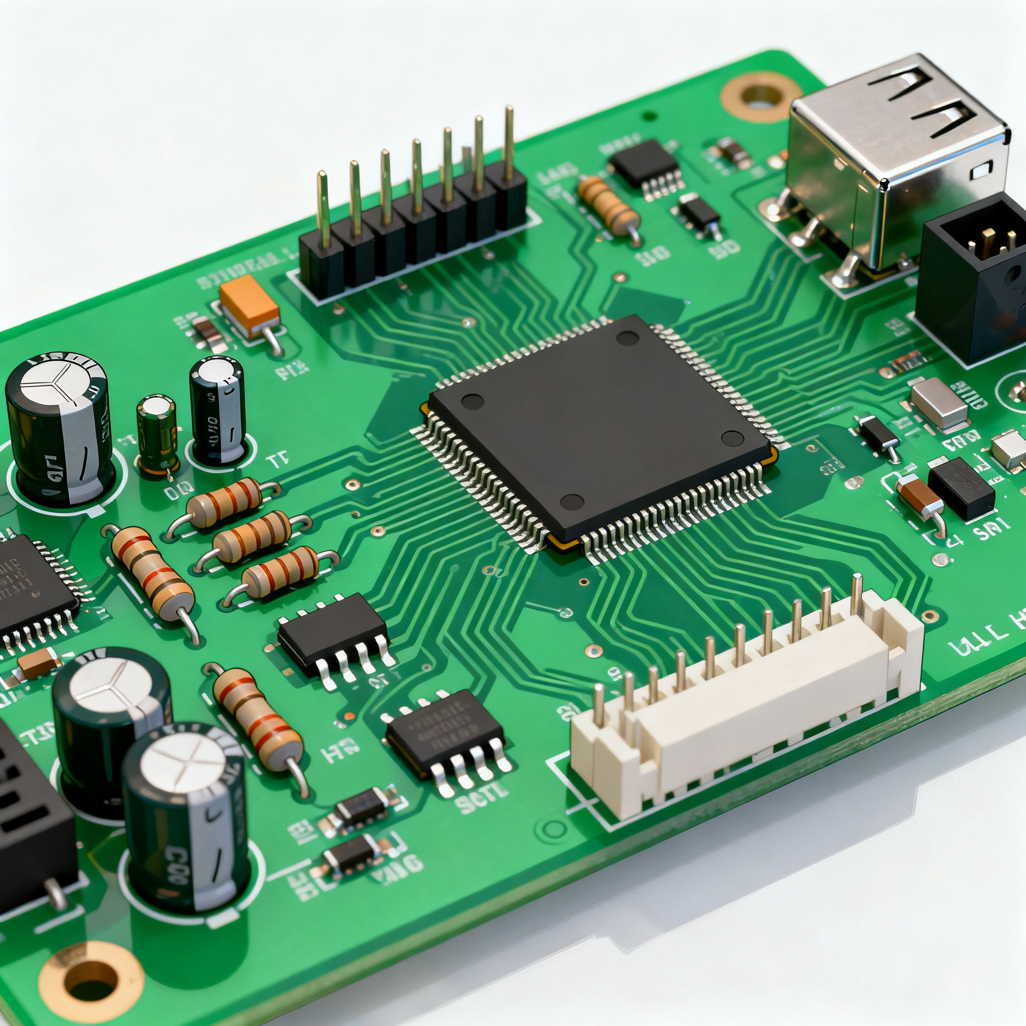
Home automation systems rely heavily on PCBs to integrate various electronic components that control lighting, climate, security, and entertainment systems. The core principles of PCB design for these applications involve ensuring signal integrity, optimizing power distribution, and minimizing electromagnetic interference (EMI). A well-designed PCB not only enhances system performance but also ensures compliance with industry standards such as IPC-A-610 and IPC-2221.
Key architectural considerations include the arrangement of layers within the PCB stackup, trace width and spacing, and the selection of materials. Each of these factors plays a critical role in maintaining signal integrity and operational reliability. Additionally, the manufacturing process must be considered to ensure cost-effectiveness and scalability.
Detailed Specifications
When designing a PCB for home automation control, several specifications must be taken into account. These include trace width, spacing, via sizes, and clearances. Adhering to these specifications ensures that the PCB can handle the necessary electrical loads and operate efficiently in various environmental conditions.
| Design Parameter | Specification | Importance |
|---|---|---|
| Trace Width | 0.25 mm | Ensures minimal resistance and heat generation |
| Trace Spacing | 0.15 mm | Prevents short circuits and maintains signal integrity |
| Via Size | 0.3 mm | Facilitates multi-layer connections |
| Clearance | 0.2 mm | Ensures isolation between conductive elements |
| Pad Size | 0.5 mm | Provides adequate area for component soldering |
| Solder Mask Clearance | 0.1 mm | Prevents solder bridging |
| Annular Ring | 0.1 mm | Ensures reliable via connections |
| Minimum Drill Size | 0.2 mm | Supports fine-pitch components |
| Aspect Ratio | 6:1 | Maintains structural integrity of vias |
| Impedance Control | ±10% | Ensures signal integrity for high-speed applications |
| Component Clearance | 1.0 mm | Facilitates assembly and rework |
| Copper Thickness | 35 µm | Supports current carrying capacity |
Key Takeaways from the Specifications
The specifications outlined in Table 1 are critical for ensuring the reliability and performance of PCBs in home automation systems. Trace width and spacing are particularly important for maintaining signal integrity and preventing electrical faults. Adequate via sizes and clearances help in achieving robust multi-layer connections while ensuring isolation between conductive elements. By adhering to these specifications, designers can minimize the risk of short circuits, enhance thermal management, and ensure compliance with industry standards.
| Layer Configuration | Application | Benefits |
|---|---|---|
| 2-Layer | Basic control circuits | Cost-effective, simple design |
| 4-Layer | Moderate complexity systems | Improved signal integrity, power distribution |
| 6-Layer | High-density interconnects | Enhanced EMI control, more routing options |
| 8-Layer | High-speed applications | Superior signal and power integrity |
| 10-Layer | Complex automation systems | Maximum routing and grounding options |
| 12-Layer | Advanced RF applications | Optimal for minimizing crosstalk, superior performance |
| 16-Layer | Extremely dense circuits | Best for critical signal integrity, extensive grounding |
| 20-Layer | Cutting-edge technology | Maximum performance, flexibility in design |
Practical Implications
The choice of layer stackup is crucial in determining the performance and reliability of home automation PCBs. A 2-layer configuration is suitable for basic control circuits where cost is a primary concern. However, as the complexity and speed of the application increase, higher layer counts become necessary. For instance, a 6-layer stackup provides enhanced EMI control, which is essential for high-density interconnects. For advanced RF applications, a 12-layer stackup offers optimal performance by minimizing crosstalk and ensuring superior signal integrity.
| Material | Dielectric Constant (Dk) | Loss Tangent (Df) |
|---|---|---|
| FR-4 | 4.5 | 0.02 |
| Rogers 4350 | 3.48 | 0.0037 |
| Rogers 4003 | 3.38 | 0.0027 |
| Polyimide | 3.5 | 0.004 |
| PTFE | 2.1 | 0.0009 |
| Ceramic | 9.8 | 0.0015 |
| BT Epoxy | 3.7 | 0.008 |
| Metal Core | 6.0 | 0.02 |
| Glass Epoxy | 4.2 | 0.015 |
| Polyester | 3.2 | 0.005 |
Application Guidelines
The selection of materials is a critical aspect of PCB design, affecting both performance and cost. FR-4 is a common choice due to its balance of cost and performance, with a dielectric constant of 4.5 and a loss tangent of 0.02. For applications requiring higher frequency operation, materials like Rogers 4350 or PTFE offer lower dielectric constants and loss tangents, enhancing signal integrity. Understanding these material properties allows designers to make informed decisions that align with the specific requirements of their home automation systems.
Design Considerations
Designing PCBs for home automation systems involves several considerations to ensure reliability and performance. One of the key aspects is signal integrity, which can be maintained by adhering to proper trace width and spacing guidelines. Additionally, selecting the appropriate layer stackup based on the complexity and speed of the application is crucial.
Thermal management is another important consideration, especially in power-intensive applications. This can be achieved through the use of thermal vias and adequate copper thickness to dissipate heat effectively. Furthermore, EMC compliance is essential to prevent interference with other electronic devices in the home. This can be addressed by incorporating shielding techniques and selecting materials with appropriate dielectric properties.
Manufacturing considerations also play a significant role in the design process. Designers must ensure that the PCB layout is compatible with the capabilities of the chosen fabrication and assembly services. This includes adhering to design for manufacturability (DFM) guidelines and selecting components that are readily available and cost-effective.
Step-by-Step Implementation
- Define Requirements: Begin by identifying the specific requirements of your home automation system, including functionality, performance, and environmental conditions.
- Select Components: Choose components that meet the defined requirements, considering factors such as power consumption, size, and cost.
- Design Schematic: Create a detailed schematic diagram that outlines the connections and interactions between components.
- Develop PCB Layout: Using the schematic, design the PCB layout, focusing on trace width, spacing, and layer stackup to ensure signal integrity and manufacturability.
- Simulate and Validate: Utilize simulation tools to validate the design, checking for potential issues such as signal interference and thermal management.
- Prototype and Test: Manufacture a prototype PCB and conduct thorough testing to identify and rectify any design flaws.
- Finalize Design: Incorporate feedback from testing to finalize the design, ensuring compliance with industry standards and manufacturing capabilities.
- Prepare Documentation: Compile comprehensive documentation, including design files, assembly instructions, and test reports, to facilitate production and maintenance.
Common Issues & Solutions
- Signal Interference: Use proper grounding techniques and shielded traces to minimize EMI and crosstalk.
- Thermal Management: Integrate thermal vias and adequate copper thickness to dissipate heat effectively.
- Component Sourcing: Select widely available components to avoid supply chain disruptions and delays.
- Manufacturing Defects: Conduct thorough DFM reviews and select reputable manufacturing partners to ensure quality production.
- Design Complexity: Simplify the design by optimizing layer stackup and minimizing unnecessary components.
- Compliance Issues: Ensure adherence to industry standards such as IPC-A-610 and IPC-2221 to avoid regulatory setbacks.
Applications & Use Cases
Home automation control PCBs are integral to a wide range of applications, from smart lighting and climate control to security systems and entertainment centers. For instance, a well-designed PCB can enhance the performance of a smart thermostat by ensuring accurate temperature readings and efficient energy management. In security systems, reliable PCBs facilitate real-time monitoring and response, providing homeowners with peace of mind.
Furthermore, the integration of IoT devices in home automation systems relies heavily on robust PCBs to handle complex data processing and communication tasks. By selecting the right components and adhering to design best practices, designers can create PCBs that support the seamless operation of these advanced systems.
Selection & Sourcing Guide
When selecting components for home automation control PCBs, consider factors such as availability, cost, and performance. Utilize online resources like IC Online to explore a wide range of electronic components and find the best options for your design. Ensure that the components meet the necessary specifications and are compatible with the chosen manufacturing processes to streamline production and reduce lead times.
FAQ
- What is the importance of trace width in PCB design? Trace width affects the current-carrying capacity and thermal performance of the PCB. Proper trace width ensures minimal resistance and heat generation, enhancing reliability.
- How do I choose the right layer stackup for my application? Consider the complexity and speed of your application. Higher layer counts offer better signal integrity and EMI control, suitable for more complex systems.
- What materials are best for high-frequency applications? Materials like Rogers 4350 and PTFE offer low dielectric constants and loss tangents, making them ideal for high-frequency applications.
- How can I ensure compliance with industry standards? Adhere to IPC design guidelines and conduct thorough testing to meet standards such as IPC-A-610 and IPC-2221.
- What are common causes of signal interference in PCBs? Poor grounding, inadequate trace spacing, and improper shielding can lead to signal interference. Address these issues through careful design and simulation.
- Why is thermal management important in PCB design? Effective thermal management prevents overheating, which can damage components and reduce the lifespan of the PCB.
- How can I simplify a complex PCB design? Optimize the layer stackup, reduce unnecessary components, and use modular design techniques to simplify complex designs.
- What should I consider when selecting a manufacturing partner? Evaluate their capabilities, quality control processes, and track record to ensure they can meet your design and production requirements.
- How do I handle component shortages? Design with flexibility in mind, allowing for alternative components, and maintain good relationships with multiple suppliers to mitigate shortages.
- What is the role of a solder mask in PCB design? A solder mask prevents solder bridging and provides protection against environmental factors, ensuring the longevity of the PCB.
Conclusion
In the realm of home automation, the reliability and performance of control systems hinge on the careful design and assembly of PCBs. By adhering to industry standards, selecting the right components, and employing robust design strategies, engineers can create PCBs that meet the demanding requirements of modern smart homes. This article has provided a comprehensive guide to the key considerations and best practices for designing PCBs for home automation control systems, paving the way for innovation and excellence in this dynamic field.