High-Speed PCB Routing Practices: Troubleshooting Common Pitfalls for Optimal Performance
High-Speed PCB Routing Practices: Troubleshooting Common Pitfalls for Optimal Performance table { border-collapse: collapse; width: 100%; margin: 20px 0; } th, td { border: 1px solid #000; padding: 8p...
Introduction
In the rapidly evolving field of electronics, high-speed PCB (Printed Circuit Board) routing has become a critical skill for engineers. As devices become more compact and complex, the need for efficient routing techniques that minimize interference and ensure signal integrity is paramount. This article explores the intricacies of high-speed PCB routing, focusing on the selection and application of integrated circuits (ICs) to optimize performance and troubleshoot common pitfalls.
Technical Overview
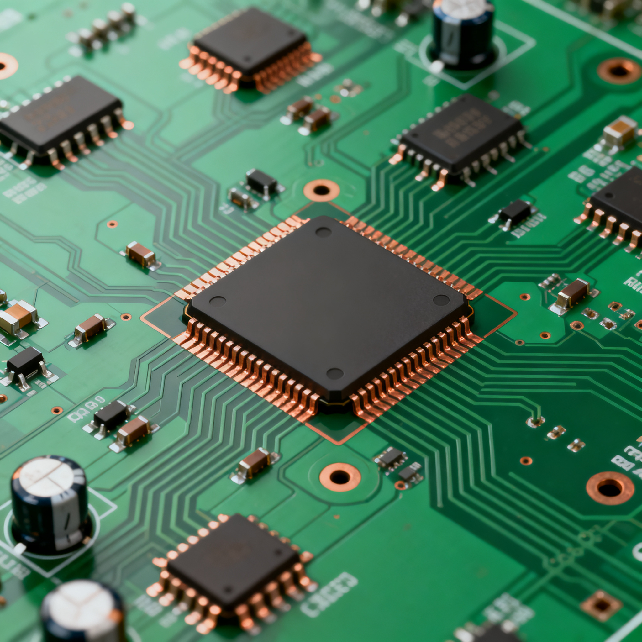
High-speed PCB routing involves the careful design and layout of circuit pathways to accommodate fast signal transmission. The architecture of a PCB is crucial, as it determines the physical placement and electrical connectivity of components. Key principles include minimizing trace lengths, maintaining consistent impedance, and reducing electromagnetic interference (EMI). The choice of ICs plays a significant role in these aspects, as their specifications dictate the electrical characteristics and performance capabilities of the circuit.
Detailed Specifications
Understanding the core specifications of ICs is essential for selecting the right component for high-speed applications. These specifications include CPU speed, memory capacity, available peripherals, power requirements, and package type. Each parameter influences the performance and suitability of the IC for specific applications.
| Specification | Value | Description |
|---|---|---|
| CPU Speed | 1.2 GHz | Maximum processing speed of the CPU |
| Memory | 512 MB | On-chip memory capacity |
| Peripherals | GPIO, UART, SPI | Available peripheral interfaces |
| Power Supply | 3.3V | Operating voltage requirement |
| Package | LQFP-64 | Physical package type |
| Flash Memory | 1 MB | On-chip flash storage |
| ADC Channels | 8 | Number of analog-to-digital converter channels |
| Temperature Range | -40°C to 85°C | Operational temperature range |
| Clock Frequency | 100 MHz | Internal clock frequency |
| I/O Pins | 48 | Number of input/output pins |
Key Takeaways from the Specifications
The specifications outlined above provide a comprehensive overview of the IC's capabilities. The CPU speed of 1.2 GHz indicates the processing power, essential for high-speed data handling. Memory and flash storage are crucial for buffering and data retention, while the range of peripherals ensures versatile connectivity options. The power supply voltage and package type are critical for compatibility with other board components. Understanding these parameters helps in selecting an IC that meets the performance and environmental requirements of the application.
| Characteristic | Value | Details |
|---|---|---|
| Operating Voltage | 3.3V | Standard voltage for operation |
| Max Current | 500 mA | Maximum current draw |
| Input Voltage Range | 2.7V - 3.6V | Acceptable input voltage range |
| Output High Voltage | 2.9V | Minimum voltage for logic high |
| Output Low Voltage | 0.4V | Maximum voltage for logic low |
| Propagation Delay | 5 ns | Time delay for signal propagation |
| Rise Time | 2 ns | Time taken for signal to rise |
| Fall Time | 2 ns | Time taken for signal to fall |
| Input Capacitance | 10 pF | Capacitance at input |
| Output Sink Current | 20 mA | Current that can be sunk by output |
| Thermal Resistance | 30°C/W | Resistance to heat flow |
Practical Implications
The electrical characteristics of an IC are vital for ensuring reliable operation in high-speed applications. The operating voltage and current specifications define the power requirements and limitations. Timing parameters such as propagation delay, rise, and fall times are crucial for maintaining signal integrity and synchronizing with other components. Understanding these characteristics helps in designing circuits that minimize power consumption and maximize performance, ensuring that the IC operates within its specified limits.
| Use Case | Configuration | Benefits |
|---|---|---|
| Embedded Systems | Single-core, 512 MB RAM | Cost-effective and efficient for basic tasks |
| IoT Devices | Low power, integrated peripherals | Energy-efficient with broad connectivity |
| Industrial Automation | High-speed I/O, robust design | Reliable operation in harsh environments |
| Consumer Electronics | High-performance CPU, rich interfaces | Enhanced user experience |
| Automotive Applications | High-temp tolerance, safety features | Safety and reliability in vehicle systems |
| Telecommunications | High-speed data processing | Efficient data handling and communication |
| Medical Devices | Precision, low noise | Accurate and reliable patient monitoring |
Application Guidelines
The application comparison table highlights the versatility of ICs in various domains. For embedded systems, a simple configuration with moderate memory suffices, while IoT devices benefit from low power and integrated peripherals. Industrial automation demands high-speed I/O and robust design, ensuring reliable performance. Consumer electronics require high-performance CPUs for enhanced user experiences, whereas automotive applications prioritize safety and temperature tolerance. Selecting the right configuration based on these criteria ensures optimal performance and cost-effectiveness in the desired application.
Design Considerations
Designing a high-speed PCB involves several critical considerations to ensure optimal performance. First and foremost is the layout of traces. Shorter trace lengths reduce inductance and capacitance, minimizing signal degradation. Maintaining consistent impedance across traces is crucial for signal integrity, especially in high-frequency applications. This often requires careful selection of trace widths and spacing, as well as the use of controlled impedance substrates.
Another key factor is the management of electromagnetic interference (EMI). Proper grounding and the strategic placement of decoupling capacitors can significantly reduce EMI, ensuring that signals remain clean and free from noise. Additionally, the use of differential signaling can further improve noise immunity, providing a robust solution for high-speed data transmission.
Thermal management is also a critical aspect of PCB design. High-speed components generate significant heat, which must be effectively dissipated to prevent damage and ensure longevity. This can be achieved through the use of heat sinks, thermal vias, and appropriate board materials with high thermal conductivity.
Finally, the selection of components, including ICs, connectors, and passive elements, must align with the overall design goals. Components should be chosen based on their electrical characteristics, package size, and compatibility with the PCB layout. By addressing these design considerations, engineers can create high-speed PCBs that deliver reliable performance and meet the demands of modern electronic applications.
Step-by-Step Implementation
- Define the Circuit Requirements: Begin by outlining the specific requirements of the circuit, including performance targets, environmental conditions, and regulatory compliance.
- Select Suitable ICs: Based on the defined requirements, choose ICs that meet the necessary specifications for speed, power, and functionality.
- Design the Schematic: Create a detailed schematic that includes all components and their interconnections, ensuring that each element is appropriately placed and connected.
- Plan the PCB Layout: Use PCB design software to lay out the traces, components, and vias, paying close attention to trace routing, impedance control, and signal integrity.
- Perform Signal Integrity Analysis: Simulate the PCB design to evaluate signal integrity, checking for issues such as reflections, crosstalk, and EMI.
- Optimize the Design: Make necessary adjustments to the layout and component selection to address any issues identified during simulation.
- Manufacture the PCB: Select a reputable PCB manufacturer that can meet the design specifications and quality standards.
- Test and Validate: Once the PCB is assembled, conduct thorough testing to validate its performance and ensure it meets all design requirements.
Common Issues & Solutions
- Signal Integrity Problems: Use controlled impedance traces and proper termination to minimize reflections and signal degradation.
- EMI Concerns: Implement shielding, grounding, and filtering techniques to reduce electromagnetic interference.
- Thermal Management: Incorporate heat sinks, thermal vias, and appropriate materials to manage heat dissipation effectively.
- Power Supply Noise: Use decoupling capacitors and voltage regulators to stabilize the power supply and reduce noise.
- Component Placement Errors: Follow best practices for component placement, ensuring that sensitive components are isolated from noise sources.
- Manufacturing Variability: Collaborate with PCB manufacturers to ensure that design tolerances are met and that quality control processes are in place.
Applications & Use Cases
High-speed PCBs are integral to a wide range of applications, from consumer electronics to industrial automation. In telecommunications, they enable efficient data transmission and processing, while in automotive systems, they provide the reliability and safety needed for critical functions. In medical devices, high-speed PCBs ensure accurate data collection and processing, contributing to effective patient monitoring. By selecting the appropriate ICs and design practices, engineers can create PCBs that meet the specific needs of each application.
Selection & Sourcing Guide
For sourcing the right ICs and components for high-speed PCB applications, consider visiting IC Online. This platform offers a wide range of components, datasheets, and selection tools to help engineers find the best solutions for their projects. Ensure that components are sourced from reputable suppliers to guarantee quality and reliability.
FAQ
- What is high-speed PCB routing? High-speed PCB routing involves designing circuit pathways that support fast signal transmission while minimizing interference and maintaining signal integrity.
- Why is impedance control important? Impedance control is crucial for maintaining signal integrity, especially in high-frequency applications, as it prevents signal reflections and degradation.
- How can I reduce EMI in my PCB design? EMI can be reduced through proper grounding, the use of decoupling capacitors, and the implementation of shielding and filtering techniques.
- What role do IC specifications play in PCB design? IC specifications determine the electrical characteristics and performance capabilities of the circuit, influencing component selection and layout design.
- What are the key considerations for thermal management? Effective thermal management involves using heat sinks, thermal vias, and high-conductivity materials to dissipate heat and prevent component damage.
- How do I ensure reliable component placement? Follow best practices for component placement, such as isolating sensitive components from noise sources and aligning them with the PCB layout.
- What tools are available for signal integrity analysis? PCB design software often includes simulation tools for evaluating signal integrity, checking for issues like reflections and crosstalk.
- How do I choose the right IC for my application? Select ICs based on their specifications, such as CPU speed, memory, and peripherals, ensuring they meet the performance and environmental requirements of the application.
- What are common pitfalls in high-speed PCB design? Common pitfalls include inadequate impedance control, poor thermal management, and insufficient EMI mitigation strategies.
- How can I ensure quality in PCB manufacturing? Collaborate with reputable PCB manufacturers, specify design tolerances, and implement quality control processes to ensure reliable production.
Conclusion
High-speed PCB routing is a complex yet essential aspect of modern electronics design. By understanding and applying best practices in IC selection, layout design, and signal integrity management, engineers can create reliable and efficient PCBs that meet the demands of today's high-speed applications. With careful consideration of specifications, electrical characteristics, and application requirements, high-speed PCBs can deliver optimal performance across a wide range of industries.