High-Speed PCB Routing Practices: Avoiding Common Pitfalls in Complex Circuits
High-Speed PCB Routing Practices: Avoiding Common Pitfalls in Complex Circuits Introduction In the fast-evolving field of electronics, high-speed PCB routing has become a critical aspect of designing ...
Introduction
In the fast-evolving field of electronics, high-speed PCB routing has become a critical aspect of designing complex circuits. With the increasing demand for faster and more efficient electronic devices, engineers must adopt advanced routing techniques to ensure optimal performance. Understanding the nuances of high-speed PCB design is essential for avoiding common pitfalls that can lead to signal integrity issues, electromagnetic interference (EMI), and overall subpar circuit performance.
Technical Overview
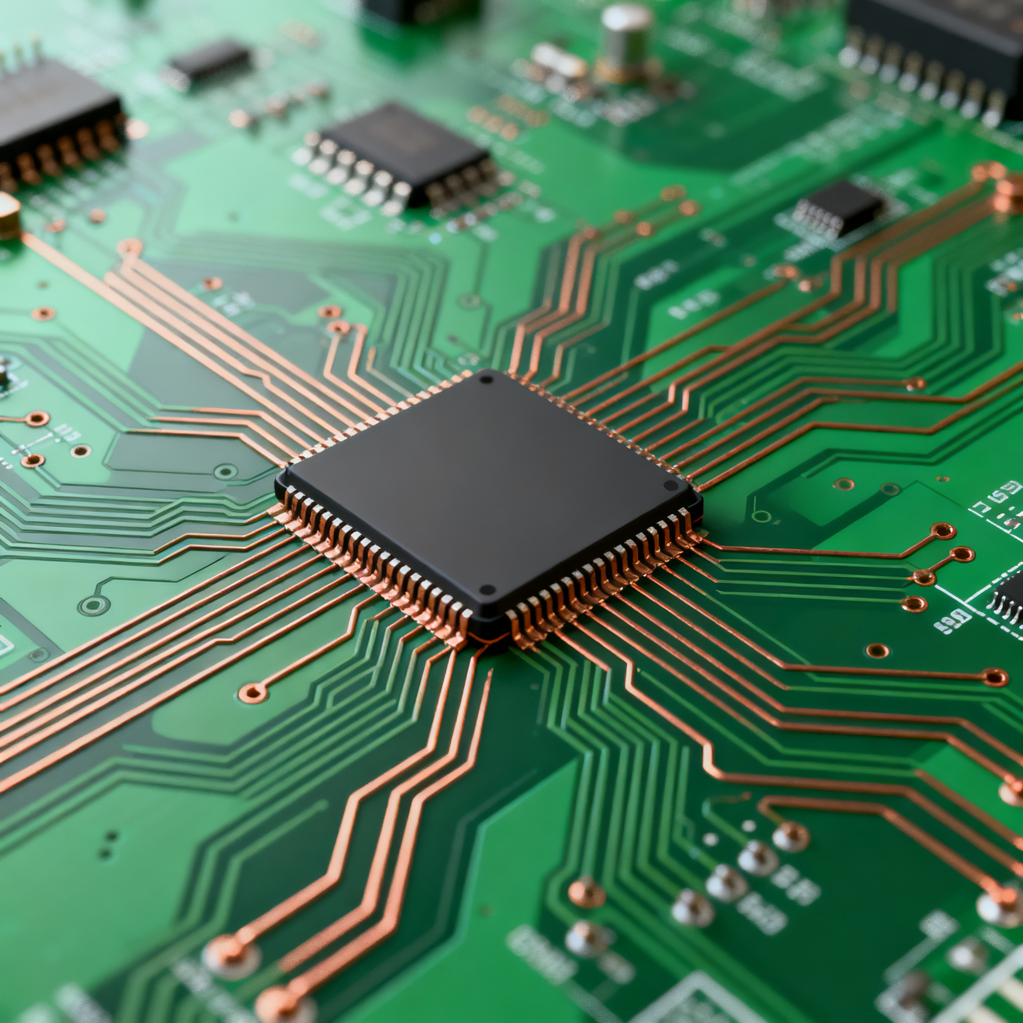
High-speed PCB routing involves the careful planning and execution of trace layouts on a printed circuit board to ensure signal integrity and minimize interference. The architecture of high-speed PCBs typically includes multiple layers to accommodate different signal types and power distribution. Key principles include impedance control, differential pair routing, and the use of ground planes to mitigate EMI. Adhering to industry standards such as IPC-2221 and IPC-A-610 is crucial for ensuring that PCBs meet quality and performance benchmarks.
Detailed Specifications
When selecting components for high-speed PCB designs, several specifications are critical. These include CPU speed, memory capacity, peripheral support, power requirements, and package types. Understanding these specifications is essential for designing circuits that meet performance and reliability goals.
| Specification | Details | Importance |
|---|---|---|
| CPU Speed | 3.2 GHz | Determines processing capability |
| Memory | 16GB DDR4 | Impacts data handling and speed |
| Peripherals | USB, HDMI, Ethernet | Expandability and connectivity |
| Power | 5V, 3.3V | Efficiency and thermal management |
| Package | LGA, BGA | Influences assembly and cooling |
| Operating Temperature | -40°C to 85°C | Environmental suitability |
| Storage Type | NAND Flash | Data retention and speed |
| Interface Type | SPI, I2C | Communication protocols |
| Clock Speed | 400 MHz | Sync timing for operations |
| GPIO | 32 Pins | Input/output versatility |
Key Takeaways from the Specifications
The core specifications outlined above are pivotal in determining the overall performance and application scope of a PCB. CPU speed and memory directly affect processing power and data throughput, essential for high-speed applications. The choice of peripherals and interface types determines the connectivity and expandability of the system. Power specifications are crucial for ensuring efficient energy use and managing thermal output, which is vital for maintaining system stability under high-load conditions. Package types like LGA and BGA impact assembly complexity and heat dissipation capabilities, influencing both manufacturing processes and operational reliability.
| Characteristic | Specification | Significance |
|---|---|---|
| Operating Voltage | 1.2V - 3.3V | Power supply range |
| Current Rating | 50mA per I/O | Current handling capability |
| Input Voltage High | 2.0V min | Logic high threshold |
| Input Voltage Low | 0.8V max | Logic low threshold |
| Output Voltage High | 2.9V min | Output drive strength |
| Output Voltage Low | 0.4V max | Output drive strength |
| Propagation Delay | 5ns | Signal timing performance |
| Rise/Fall Time | 2ns | Signal edge rate |
| Input Capacitance | 5pF | Impact on signal integrity |
| Output Impedance | 50Ω | Impedance matching |
| Power Dissipation | 500mW | Thermal performance |
| ESD Protection | 2kV HBM | Robustness against static discharge |
Practical Implications
The electrical characteristics of a component are crucial for ensuring that it functions correctly within a circuit. Operating voltage and current ratings define the power requirements and handling capabilities, which impact the choice of power supply and regulators. Propagation delay and rise/fall times are critical for high-speed applications, affecting signal integrity and synchronization across the PCB. Input and output voltage levels dictate the compatibility with other components, ensuring reliable logic levels are maintained. ESD protection levels are vital for safeguarding against electrostatic discharge, which can damage sensitive components.
| Application | Configuration | Benefits |
|---|---|---|
| Consumer Electronics | Standard PCB with HDMI, USB | High connectivity, ease of use |
| Automotive Systems | Robust PCB with CAN Bus | Reliability, real-time data |
| Industrial Automation | Multi-layer PCB with Ethernet | Durability, high-speed data |
| Medical Devices | Compact PCB with SPI/I2C | Precision, low power |
| Telecommunications | High-frequency PCB with RF modules | Wide bandwidth, low latency |
| Aerospace | Radiation-hardened PCB | Extreme environment suitability |
| IoT Devices | Low-power PCB with Wi-Fi/Bluetooth | Connectivity, battery efficiency |
Application Guidelines
The application comparison table illustrates the diverse use cases of high-speed PCB designs across various industries. For consumer electronics, the emphasis is on connectivity and user-friendliness, while automotive systems prioritize reliability and real-time communication. Industrial automation demands durable PCBs capable of handling high-speed data transfer. In contrast, medical devices focus on precision and power efficiency. Each application requires specific configurations to meet unique demands, highlighting the importance of selecting the right components and design practices for each scenario.
Design Considerations
Designing high-speed PCBs requires careful attention to several critical factors to ensure optimal performance. First, consider the impedance control; maintaining consistent impedance across traces helps minimize reflections and signal loss. Implementing differential pair routing for high-speed signals can reduce EMI and improve signal integrity. Ground planes are essential for providing a stable reference and minimizing interference. Additionally, trace length matching is crucial for ensuring synchronized signal arrival, particularly in applications with parallel data paths.
Thermal management is another vital consideration. Efficient heat dissipation can be achieved through proper component placement, the use of heat sinks, and thermal vias. Power distribution networks must be designed to minimize voltage drops and ensure stable power delivery to all components. Finally, adhering to industry standards and guidelines, such as those provided by IPC, is essential for ensuring quality and reliability in high-speed PCB designs.
Step-by-Step Implementation
- Define the PCB requirements based on the application, including speed, power, and connectivity needs.
- Select appropriate components that meet the specifications outlined in the datasheets, focusing on electrical and thermal characteristics.
- Design the schematic, ensuring all components are correctly placed and connections are logically routed.
- Layout the PCB, paying close attention to trace impedance, differential pair routing, and ground plane implementation.
- Perform signal integrity analysis to identify potential issues with reflections, crosstalk, and EMI.
- Optimize the power distribution network to minimize voltage drops and ensure stable power delivery.
- Prototype the design and conduct thorough testing to validate performance against specifications.
- Iterate on the design as necessary, addressing any issues identified during testing to improve reliability and performance.
Common Issues & Solutions
- Issue: Signal Integrity Problems
Solution: Implement impedance control and differential pair routing. - Issue: Electromagnetic Interference (EMI)
Solution: Use ground planes and shielded traces. - Issue: Thermal Management Challenges
Solution: Optimize component placement and use thermal vias. - Issue: Power Distribution Issues
Solution: Design robust power distribution networks with adequate decoupling capacitors. - Issue: Component Compatibility
Solution: Verify voltage levels and interface types for compatibility. - Issue: Manufacturing Variability
Solution: Adhere to IPC standards and conduct thorough quality inspections.
Applications & Use Cases
High-speed PCB designs are integral to numerous applications across various industries. In telecommunications, they enable high-bandwidth data transmission with minimal latency. Consumer electronics benefit from high-speed PCBs through enhanced connectivity and performance, allowing for seamless integration with multiple devices. Automotive systems rely on robust PCB designs for real-time data processing and communication, essential for advanced driver-assistance systems (ADAS) and infotainment. In the medical field, precision and reliability are paramount, with high-speed PCBs supporting critical diagnostic and monitoring equipment.
Selection & Sourcing Guide
When selecting components for high-speed PCB designs, it is crucial to consult detailed datasheets and adhere to industry standards. A reliable sourcing option is IC Online, a comprehensive resource for finding components that meet specific performance criteria. Ensure components are sourced from reputable manufacturers to guarantee quality and reliability.
FAQ
- What is the importance of impedance control in high-speed PCB designs?
Impedance control is vital for minimizing signal reflections and ensuring signal integrity, particularly in high-frequency applications. - How can I reduce electromagnetic interference (EMI) in my PCB design?
Implementing ground planes, differential pair routing, and proper shielding can significantly reduce EMI. - What are the key considerations for thermal management in high-speed PCBs?
Efficient heat dissipation can be achieved through strategic component placement, the use of heat sinks, and thermal vias. - How do I ensure power distribution network reliability?
Design robust power distribution networks with sufficient decoupling capacitors to minimize voltage drops and ensure stable power delivery. - Why is trace length matching important?
Trace length matching ensures synchronized signal arrival, which is crucial for maintaining data integrity in parallel data paths. - What are the benefits of using differential pair routing?
Differential pair routing helps reduce EMI and improve signal integrity by maintaining balanced signal paths. - How can I verify component compatibility?
Check voltage levels and interface types in datasheets to ensure compatibility between components. - What standards should I follow for high-speed PCB design?
Adhere to IPC standards such as IPC-2221 and IPC-A-610 for quality and performance assurance.
Conclusion
High-speed PCB routing is a complex yet essential aspect of modern electronics design. By understanding and applying key principles such as impedance control, differential pair routing, and effective thermal management, engineers can avoid common pitfalls and achieve optimal performance. Adhering to industry standards and carefully selecting components based on detailed specifications are crucial steps in creating reliable and efficient circuits that meet the demands of today's advanced applications.