High-Speed PCB Routing Practices: Avoiding Common Pitfalls for Optimal Signal Integrity
High-Speed PCB Routing Practices: Avoiding Common Pitfalls for Optimal Signal Integrity body { font-family: Arial, sans-serif; line-height: 1.6; margin: 0; padding: 20px; } h2 { color: #333; margin-to...
Introduction
In today's fast-evolving electronics industry, the demand for high-speed printed circuit boards (PCBs) is ever-increasing. As devices become more sophisticated, ensuring optimal signal integrity becomes crucial. High-speed PCB routing is a critical aspect of PCB design, as it directly impacts the performance and reliability of electronic devices. Understanding component specifications, datasheets, and application circuits is essential for engineers to make informed decisions and avoid common pitfalls.
Technical Overview
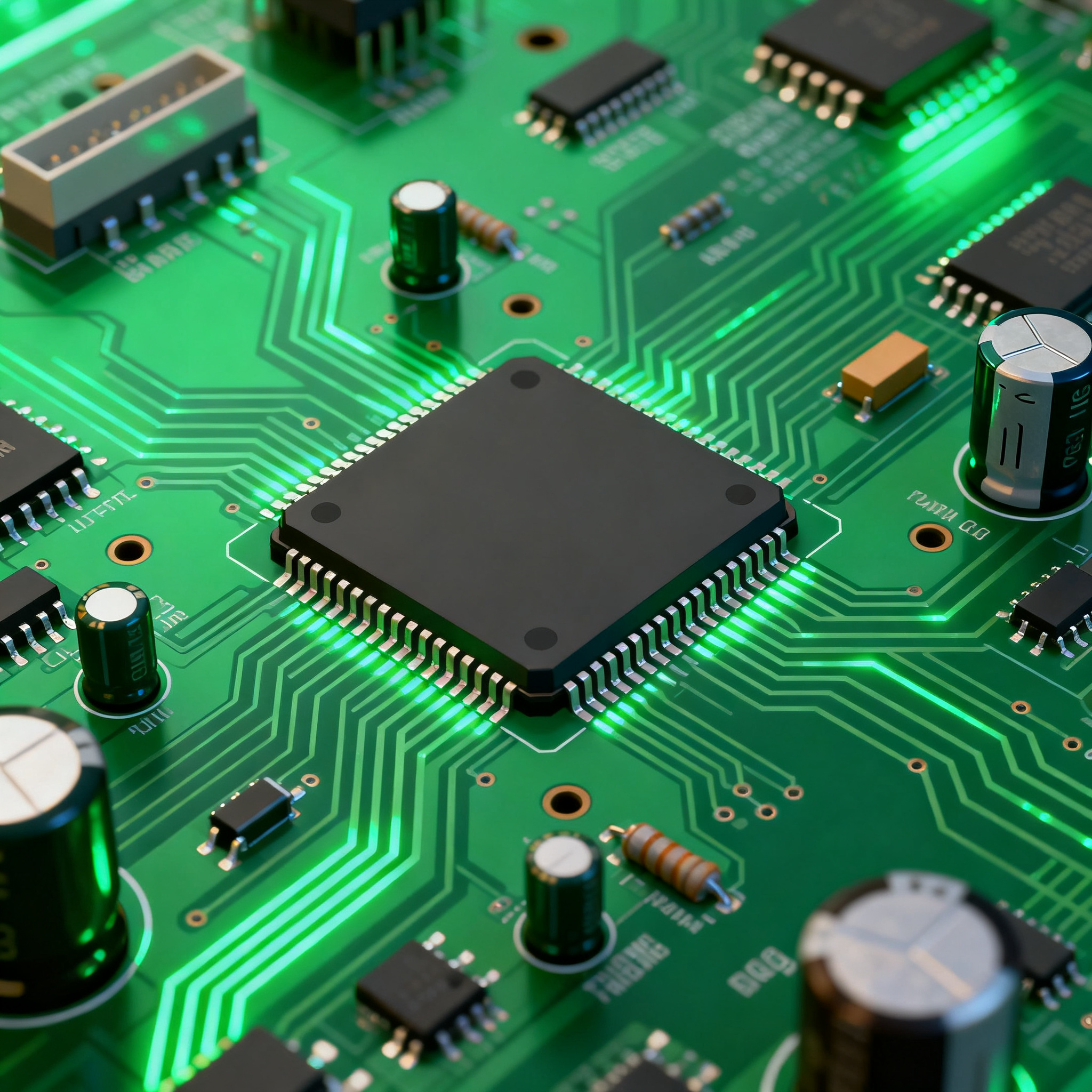
High-speed PCB routing involves designing PCB traces that can handle high-frequency signals without significant signal degradation. This requires a deep understanding of the core concepts such as impedance matching, signal integrity, and electromagnetic interference (EMI). The architecture of high-speed PCBs often includes multi-layered boards, controlled impedance traces, and differential pairs to manage these challenges effectively. Key principles include minimizing trace lengths, avoiding sharp angles, and ensuring proper grounding. Adhering to IPC standards, such as IPC-2221 for PCB design and IPC-A-610 for quality inspection, is vital for achieving optimal results.
Detailed Specifications
When selecting components for high-speed PCB routing, certain specifications are paramount. These include CPU speed, memory capacity, power requirements, and package type. Understanding these specifications helps in choosing the right components that align with the desired performance and reliability of the PCB.
| Specification | Details | Comments |
|---|---|---|
| CPU Speed | 3.2 GHz | High-speed processing capability |
| Memory | 16 GB DDR4 | Supports high bandwidth |
| Peripherals | USB 3.1, HDMI 2.0 | Provides various connectivity options |
| Power | 5V, 3A | Efficient power consumption |
| Package | BGA | Compact design for space-saving |
| Operating Temperature | -40°C to 85°C | Wide temperature range |
| Storage Temperature | -55°C to 125°C | Ensures durability |
| Dimensions | 35mm x 35mm | Small footprint |
| Weight | 10 grams | Lightweight for portable applications |
| Life Cycle | 10 years | Long-term availability |
Key Takeaways from the Specifications
The specifications provided in the table highlight the critical aspects of component selection for high-speed PCBs. A CPU speed of 3.2 GHz ensures that the system can handle high-performance tasks efficiently. The 16 GB DDR4 memory supports significant data throughput, crucial for applications requiring rapid data processing. The BGA package offers a compact design, making it ideal for space-constrained applications. Additionally, the wide operating temperature range and long life cycle ensure reliability and durability in various environments.
| Characteristic | Value | Significance |
|---|---|---|
| Voltage | 1.8V to 3.3V | Supports low power applications |
| Current | 500mA | Efficient current handling |
| Timing | 10ns rise/fall time | Fast signal transitions |
| I/O Voltage | 3.3V | Standard I/O interface level |
| Input Capacitance | 5pF | Low input loading |
| Output Drive Strength | 15mA | Strong signal drive capability |
| ESD Protection | 2kV | Robust against electrostatic discharge |
| Thermal Resistance | 25°C/W | Efficient heat dissipation |
| Noise Margin | 0.4V | High noise immunity |
| Propagation Delay | 5ns | Low latency for high-speed applications |
Practical Implications
The electrical characteristics outlined in the table are essential for maintaining signal integrity in high-speed PCBs. The voltage range of 1.8V to 3.3V is suitable for low-power applications, while the current rating of 500mA ensures efficient power distribution. The timing parameters, such as a 10ns rise/fall time, indicate the ability to handle fast signal transitions, crucial for high-frequency applications. The strong output drive strength and ESD protection enhance the robustness and reliability of the PCB in various operating conditions.
| Use Case | Configuration | Benefits |
|---|---|---|
| Consumer Electronics | Standard Configuration | Cost-effective and efficient |
| Industrial Automation | Robust Configuration | High reliability in harsh conditions |
| Telecommunications | High-Speed Configuration | Optimized for data throughput |
| Automotive Systems | Temperature-Resistant Configuration | Ensures performance in extreme temperatures |
| Medical Devices | Precision Configuration | High accuracy and reliability |
| IoT Applications | Low-Power Configuration | Extended battery life |
Application Guidelines
The application comparison table illustrates the versatility of high-speed PCBs across different industries. In consumer electronics, a standard configuration offers a cost-effective solution, while industrial automation benefits from a robust configuration capable of withstanding harsh environments. Telecommunications demand high-speed configurations for optimal data throughput. Automotive systems require temperature-resistant configurations to ensure reliability in extreme conditions. Medical devices prioritize precision and reliability, while IoT applications benefit from low-power configurations for extended battery life.
Design Considerations
When designing high-speed PCBs, several key considerations must be taken into account to ensure optimal performance and signal integrity. Here are some practical design guidelines:
- Impedance Control: Proper impedance matching is crucial to minimize signal reflections and losses. Utilize controlled impedance traces and differential pairs where necessary.
- Trace Length: Minimize trace lengths to reduce signal delay and crosstalk. Use meandering or serpentine traces to match trace lengths in differential pairs.
- Grounding: Implement a solid ground plane to provide a low-impedance path for return currents and minimize EMI.
- Signal Isolation: Separate high-speed signals from noisy power and ground planes to prevent interference.
- Via Management: Limit the use of vias, as they can introduce inductance and affect signal integrity. Consider using blind or buried vias for multi-layer boards.
- Termination: Apply proper termination techniques, such as series or parallel termination, to reduce signal reflections at the end of transmission lines.
- Power Distribution: Use wide power traces and decoupling capacitors to ensure stable power supply to all components.
- Simulation and Testing: Utilize simulation tools to model and analyze signal integrity issues before fabrication. Conduct thorough testing to verify performance.
Step-by-Step Implementation
Implementing high-speed PCB routing requires careful planning and execution. Follow these detailed steps to ensure success:
- Define Requirements: Identify the performance and functionality requirements for your PCB, including speed, power, and environmental conditions.
- Select Components: Choose components that meet the defined specifications and are suitable for high-speed applications. Refer to datasheets and application notes for guidance.
- Create Schematic: Design a detailed schematic, ensuring correct component placement and connectivity. Use schematic capture software for accuracy.
- Layout Design: Begin the PCB layout process, focusing on trace routing, layer stackup, and component placement. Prioritize critical signal paths first.
- Impedance Matching: Calculate and implement controlled impedance traces for high-speed signals. Use simulation tools to verify impedance values.
- Grounding and Power: Establish a solid ground plane and design an efficient power distribution network. Place decoupling capacitors near power pins.
- Signal Integrity Analysis: Perform signal integrity analysis using simulation tools to identify potential issues such as crosstalk and reflections.
- Review and Verify: Conduct a thorough design review, checking for errors and compliance with standards. Verify design against the initial requirements.
- Prototype and Test: Manufacture a prototype PCB and conduct testing to validate performance. Identify and resolve any issues before mass production.
- Documentation: Prepare comprehensive documentation, including design files, test results, and assembly instructions, for future reference and production.
Common Issues & Solutions
High-speed PCB routing can present several challenges. Here are some common issues and their solutions:
- Signal Reflections: Reflections occur when impedance is not matched. Use proper termination techniques to minimize reflections.
- Crosstalk: Crosstalk arises from closely spaced traces. Increase trace spacing and use ground planes to reduce crosstalk.
- EMI Interference: Electromagnetic interference can degrade signal quality. Implement shielding and maintain proper grounding to mitigate EMI.
- Power Integrity Issues: Voltage drops and noise in power distribution can affect performance. Use wide power traces and adequate decoupling capacitors.
- Thermal Management: Excessive heat can damage components. Design efficient thermal management solutions, such as heat sinks and thermal vias.
- Manufacturing Variability: Variations in manufacturing processes can impact performance. Work closely with manufacturers and specify clear design rules.
Applications & Use Cases
High-speed PCBs are integral to various applications, each with unique requirements:
- Consumer Electronics: Smartphones, tablets, and laptops benefit from high-speed PCBs for fast processing and connectivity.
- Industrial Automation: High-speed PCBs enable real-time control and monitoring in automated systems and robotics.
- Telecommunications: Networking equipment relies on high-speed PCBs for rapid data transmission and processing.
- Automotive Systems: Advanced driver assistance systems (ADAS) and infotainment require high-speed PCBs for reliable performance.
- Medical Devices: Diagnostic and monitoring equipment use high-speed PCBs for accurate data acquisition and processing.
Selection & Sourcing Guide
When selecting and sourcing components for high-speed PCBs, consider the following:
- Refer to IC Online for a comprehensive database of components and suppliers.
- Choose reputable manufacturers with a track record of quality and reliability.
- Verify component availability and lead times to ensure timely production.
- Consider cost, performance, and compatibility with your design requirements.
- Utilize component evaluation boards and samples for testing and validation.
FAQ
Here are some frequently asked questions about high-speed PCB routing:
- What is the importance of controlled impedance in high-speed PCBs?
Controlled impedance ensures signal integrity by minimizing reflections and losses, crucial for high-frequency applications. - How can I reduce EMI in my PCB design?
Implementing proper grounding, shielding, and trace separation can significantly reduce electromagnetic interference. - What are differential pairs, and why are they used?
Differential pairs consist of two traces carrying equal and opposite signals, reducing noise and improving signal integrity. - How do I choose the right PCB material for high-speed applications?
Select materials with low dielectric constant and loss tangent to minimize signal attenuation and distortion. - What role do decoupling capacitors play in PCB design?
Decoupling capacitors stabilize power supply voltage by filtering noise and providing transient current. - How can I verify my PCB design before manufacturing?
Use simulation tools to analyze signal integrity, power integrity, and thermal performance before prototyping. - What are the best practices for routing high-speed signals?
Minimize trace lengths, use controlled impedance, and maintain proper grounding to ensure signal integrity. - How can I manage heat dissipation in high-speed PCBs?
Incorporate heat sinks, thermal vias, and proper airflow to manage heat and prevent component damage. - What are the challenges of multi-layer PCB design?
Multi-layer designs require careful planning of layer stackup, via management, and signal integrity analysis. - Why is documentation important in PCB design?
Comprehensive documentation ensures clear communication with manufacturers and facilitates future design iterations.
Conclusion
High-speed PCB routing is a complex but essential aspect of modern electronics design. By understanding component specifications, electrical characteristics, and application requirements, engineers can create reliable and efficient PCBs that meet industry standards. Adhering to best practices in design and implementation ensures optimal signal integrity, paving the way for innovative and high-performance electronic devices.