High-Speed Materials for PCB: A Guide to Selecting the Right Dielectrics for 5G Applications
High-Speed Materials for PCB: A Guide to Selecting the Right Dielectrics for 5G Applications Introduction With the advent of 5G technology, the demand for high-speed materials in printed circuit board...
Introduction
With the advent of 5G technology, the demand for high-speed materials in printed circuit boards (PCBs) has increased significantly. These materials are crucial for ensuring that PCBs can handle the higher frequencies and faster data rates associated with 5G applications. Selecting the right dielectrics is essential for optimizing performance and reliability in these advanced communication systems. This guide offers an in-depth look at the core specifications, electrical characteristics, and application comparisons of components used in high-speed PCB design, focusing on the specific needs of 5G technology.
Technical Overview
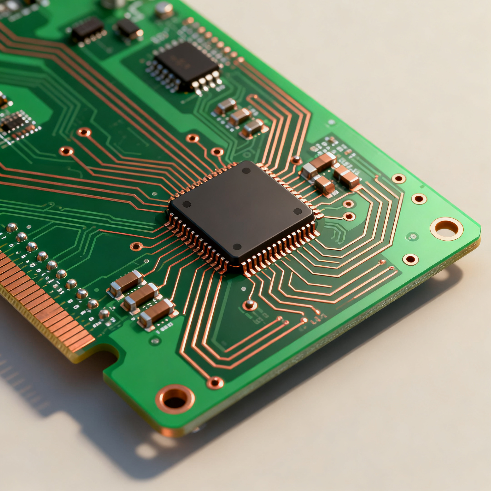
The transition to 5G technology requires a reevaluation of PCB materials and design methodologies. High-speed PCBs must support increased signal integrity, reduced electromagnetic interference (EMI), and enhanced thermal management. Key architectural considerations include the choice of dielectric materials, which directly impact the PCB's ability to handle high frequencies and fast data transmission. Dielectric constant (Dk) and dissipation factor (Df) are critical parameters that influence signal velocity and loss. Additionally, factors such as copper roughness, layer stack-up, and trace geometry play significant roles in the overall performance of high-speed PCBs.
High-speed materials for PCBs are typically characterized by low Dk and Df values, which help minimize signal distortion and power loss. These materials often include advanced composites, ceramics, and specialized laminates designed to meet the stringent requirements of 5G applications. Furthermore, adherence to standards such as IPC-2221 and IPC-4101 ensures that PCBs meet industry benchmarks for quality and performance.
Detailed Specifications
In high-speed PCB design, understanding core specifications is crucial for selecting the right components. Key specifications include CPU speed, memory capacity, peripheral compatibility, power requirements, and packaging options. These factors determine how well a PCB can support the high data rates and low latency demanded by 5G applications.
| Specification | Description | Value |
|---|---|---|
| CPU Speed | Maximum processing speed supported | 3.2 GHz |
| Memory Capacity | Total available memory | 16 GB |
| Peripheral Compatibility | Supported peripheral interfaces | USB 3.1, PCIe |
| Power Requirements | Operating voltage and current | 5V, 2A |
| Package Type | Physical packaging of the component | BGA |
| Thermal Management | Heat dissipation capabilities | Passive |
| Signal Integrity | Ability to maintain signal quality | High |
| Layer Count | Number of layers in the PCB | 8 |
| Material Type | Base material used in PCB | FR-4 |
| Dielectric Constant | Relative permittivity of the material | 3.5 |
Key Takeaways from the Specifications
The core specifications table provides insights into the fundamental attributes of high-speed PCBs designed for 5G applications. The CPU speed and memory capacity highlight the processing power and data handling capabilities necessary for high-performance tasks. Peripheral compatibility ensures that the PCB can interface with various devices, while power requirements indicate the necessary electrical input. The package type, such as BGA, influences the component's physical footprint and thermal management. Understanding these specifications is vital for engineers to design PCBs that meet the rigorous demands of 5G technology.
| Electrical Parameter | Description | Value |
|---|---|---|
| Operating Voltage | Nominal voltage for operation | 3.3V |
| Current Consumption | Average current usage | 500mA |
| Signal Rise Time | Time taken for signal to rise | 200ps |
| I/O Voltage Levels | Input/Output voltage range | 0-3.3V |
| Leakage Current | Current leakage in standby mode | 10uA |
| Switching Frequency | Frequency of signal switching | 1 GHz |
| Impedance Control | Management of signal impedance | 50 Ohms |
| Power Dissipation | Heat generated during operation | 1.5W |
| Capacitance | Capacitance of the component | 10pF |
| Inductance | Inductance value of the component | 2nH |
Practical Implications
The electrical characteristics table outlines critical parameters that affect the performance and efficiency of high-speed PCBs in 5G applications. Operating voltage and current consumption are crucial for power management, while signal rise time and switching frequency impact data transmission speed. I/O voltage levels and impedance control ensure seamless integration with other components. Understanding these characteristics allows engineers to optimize PCB designs for minimal power loss and maximum signal integrity, which are essential for reliable 5G communication.
| Application | Configuration | Use Case |
|---|---|---|
| Base Station | High power, multi-layer | Signal processing |
| Mobile Device | Compact, low power | Data transmission |
| IoT Device | Low power, high connectivity | Remote monitoring |
| Automotive | Robust, high-speed | Vehicle communication |
| Industrial Automation | Durable, high bandwidth | Process control |
| Smart Home | Energy-efficient, wireless | Home automation |
Application Guidelines
The application comparison table highlights how different configurations of high-speed PCBs cater to specific use cases. Base stations require high power and multi-layer configurations for efficient signal processing, while mobile devices demand compact and low-power designs for effective data transmission. IoT devices prioritize connectivity and low power for remote monitoring, whereas automotive applications need robust, high-speed PCBs for vehicle communication. Each application has unique requirements, guiding engineers in selecting the appropriate PCB materials and designs to achieve optimal performance in 5G environments.
Design Considerations
Designing high-speed PCBs for 5G applications involves several critical considerations to ensure optimal performance and reliability. Engineers must focus on minimizing signal loss and interference, which can be achieved by selecting materials with low dielectric constant and dissipation factor. The choice of substrate material, such as Rogers or Taconic, can significantly impact signal integrity. Additionally, careful attention should be paid to trace geometry and spacing to prevent crosstalk and impedance mismatches.
Thermal management is another crucial aspect, as high-speed components tend to generate significant heat. Implementing efficient heat dissipation mechanisms, such as heat sinks or thermal vias, can help maintain component performance and longevity. Furthermore, adherence to industry standards, such as IPC-2221, ensures that designs meet established guidelines for quality and performance.
Engineers must also consider the manufacturing capabilities of their chosen PCB fabricator. Understanding the fabricator's design rules, such as minimum trace width and spacing, helps in creating manufacturable designs that align with production capabilities. Collaboration with fabricators early in the design process can mitigate potential issues and streamline the transition from design to production.
Step-by-Step Implementation
- Requirement Analysis: Begin by defining the specific requirements for the 5G application, including frequency range, data rates, and environmental conditions.
- Material Selection: Choose appropriate dielectric materials with low Dk and Df values to minimize signal loss and distortion.
- Design Layout: Create a detailed PCB layout, focusing on trace geometry, layer stack-up, and impedance control to maintain signal integrity.
- Thermal Management: Implement thermal management solutions, such as heat sinks or thermal vias, to dissipate heat effectively.
- Simulation and Testing: Use simulation tools to validate the design and identify potential issues. Conduct thorough testing to ensure compliance with performance standards.
- Prototype Development: Develop a prototype to evaluate real-world performance and make necessary design adjustments.
- Manufacturing Collaboration: Work closely with PCB fabricators to ensure the design aligns with manufacturing capabilities and standards.
- Final Validation: Perform final validation tests to confirm that the PCB meets all specified requirements and functions as intended in the 5G application.
Common Issues & Solutions
- Signal Loss: Use low-loss dielectric materials and optimize trace geometry to reduce signal attenuation.
- EMI Interference: Implement shielding techniques and maintain proper grounding to minimize electromagnetic interference.
- Thermal Management: Incorporate heat sinks and thermal vias to dissipate heat and prevent component overheating.
- Impedance Mismatch: Design traces with controlled impedance and use proper termination techniques to avoid signal reflection.
- Crosstalk: Increase trace spacing and use differential pair routing to reduce crosstalk between adjacent signals.
- Manufacturing Constraints: Collaborate with fabricators to ensure the design complies with manufacturing capabilities and tolerances.
Applications & Use Cases
High-speed PCBs are integral to various 5G applications, each with unique demands. In telecommunications, they form the backbone of base stations, enabling efficient signal processing and data transmission. In consumer electronics, they power mobile devices, facilitating high-speed internet access and seamless connectivity. Automotive applications leverage high-speed PCBs for advanced communication systems, enhancing vehicle-to-vehicle and vehicle-to-infrastructure communication. Industrial automation relies on these PCBs for process control and monitoring, ensuring efficient and reliable operations. The versatility and performance of high-speed PCBs make them indispensable in the rapidly evolving landscape of 5G technology.
Selection & Sourcing Guide
When selecting high-speed materials for PCBs, engineers should consider factors such as dielectric constant, dissipation factor, and thermal properties. Collaborating with reputable suppliers and manufacturers is crucial for sourcing quality materials that meet the specific requirements of 5G applications. For comprehensive sourcing options and detailed component specifications, visit IC Online.
FAQ
- What are the key characteristics of high-speed PCB materials? High-speed PCB materials are characterized by low dielectric constant and dissipation factor, which help minimize signal loss and distortion.
- Why is thermal management important in high-speed PCBs? Thermal management is crucial because high-speed components generate significant heat, which can affect performance and reliability if not properly managed.
- What role does trace geometry play in PCB design? Trace geometry affects signal integrity and impedance control, which are critical for maintaining high-speed data transmission and minimizing losses.
- How does impedance control impact PCB performance? Impedance control ensures that signal paths are matched to prevent reflections and signal degradation, which is vital for high-frequency applications.
- What are some common challenges in high-speed PCB design? Common challenges include signal loss, EMI interference, thermal management, impedance mismatch, and crosstalk.
- How can engineers mitigate crosstalk in PCB designs? Engineers can mitigate crosstalk by increasing trace spacing, using differential pair routing, and implementing proper grounding techniques.
- What standards should be followed in high-speed PCB design? Engineers should adhere to standards such as IPC-2221 and IPC-4101 to ensure quality and performance benchmarks are met.
- Why is collaboration with fabricators important? Collaborating with fabricators ensures that designs align with manufacturing capabilities and helps identify potential issues early in the process.
- What simulation tools are used in PCB design? Simulation tools such as SPICE and HFSS are commonly used to validate designs and predict performance in high-speed PCB applications.
- How do high-speed PCBs benefit 5G technology? High-speed PCBs support the higher frequencies and faster data rates required by 5G applications, enabling reliable and efficient communication.
Conclusion
In conclusion, selecting the right high-speed materials for PCBs is critical for the success of 5G applications. By understanding core specifications, electrical characteristics, and application requirements, engineers can design PCBs that meet the demanding needs of modern communication systems. Careful consideration of material properties, thermal management, and manufacturing capabilities ensures that high-speed PCBs deliver optimal performance and reliability in the rapidly evolving 5G landscape.