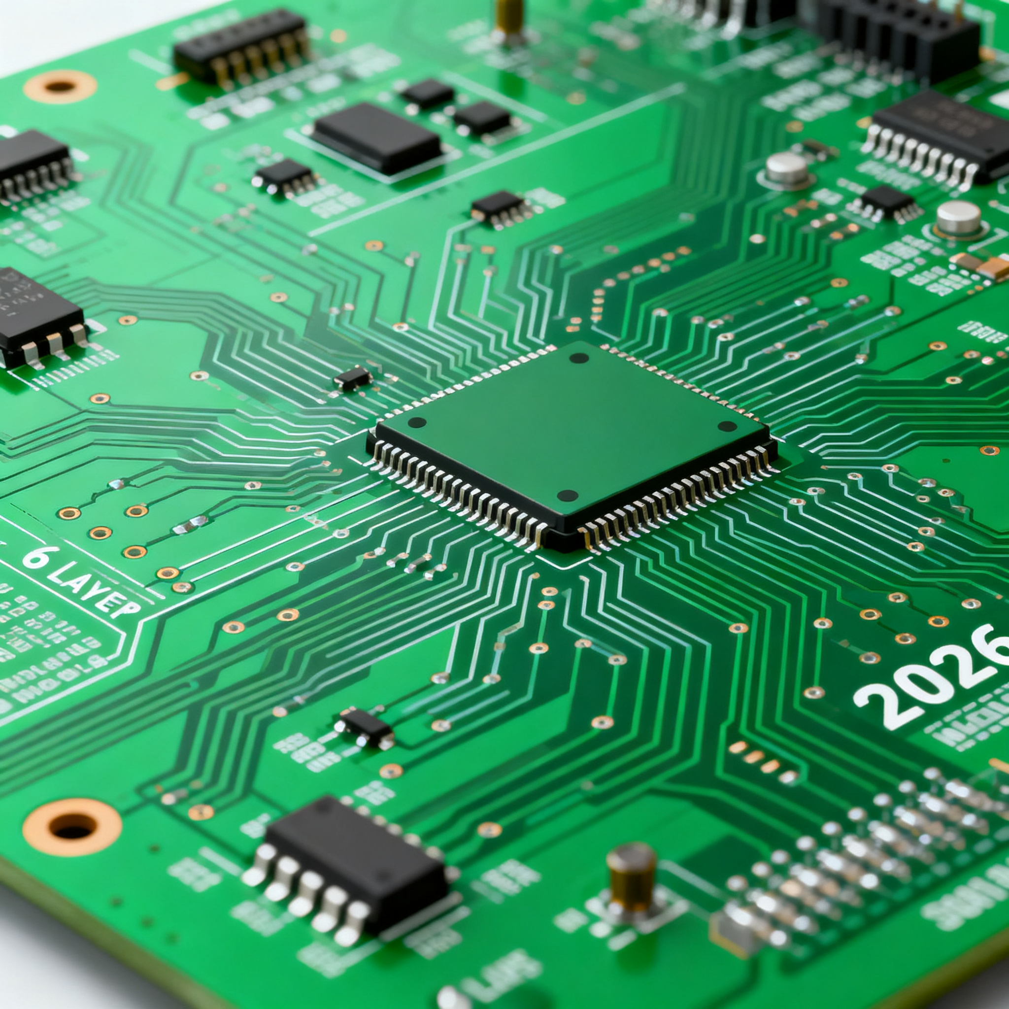
High-Density PCB Layout Best Practices to Future-Proof 6-Layer Designs for 2026 Manufacturing Trends
Why 2026's Miniaturization Surge Demands a Rethink of 6-Layer Layout Foundations You've probably noticed the shift already. Component pitches that were comfortably 0.8 mm two years ago are now 0.4 mm ...
Why 2026's Miniaturization Surge Demands a Rethink of 6-Layer Layout Foundations
You've probably noticed the shift already. Component pitches that were comfortably 0.8 mm two years ago are now 0.4 mm and shrinking. BGA ball counts are climbing past 400 on packages no larger than a postage stamp. And the design rules you relied on for 4-layer boards in 2020 simply no longer close timing or meet impedance targets. As 2026 approaches, the pressure to pack more functionality into smaller footprints — driven by wearables with multi-sensor fusion, automotive radar modules, and IoT edge nodes that must process AI inference locally — means 6-layer designs have become the new baseline for high-density interconnect. But a 6-layer board isn't immune to failure when old layout habits carry over.
The mismatch shows up in predictable ways. You route a 50 Ω trace on an outer layer, only to discover during first-article testing that impedance swings 8 Ω high because the reference plane gap beneath it was never modeled in your stack-up tool. You place bypass capacitors 2 mm from their BGA pads because "that's what worked on the 4-layer revision," and suddenly your power integrity simulation shows 120 mV of ripple where 40 mV was budgeted. These aren't hypothetical scenarios — they're the direct result of applying pre-HDI design methodologies to boards that now require controlled-impedance routing on every layer, microvia transitions, and PDN impedance below 0.1 Ω out to 100 MHz.
Following IPC-2221 design guides for conductor spacing and annular ring requirements provides a solid starting point, but the standard alone won't save you from the manufacturing realities of 2026. That's where early collaboration with an assembly partner becomes critical. Nova PCBA engineers routinely flag impedance discontinuities and via reliability risks during DFM reviews — problems that, caught late, trigger board respins costing weeks of schedule and thousands in expedited tooling. The lesson from the field is clear: a 6-layer high-density layout succeeds not when you follow a checklist, but when you understand the physical mechanisms — return current paths, glass-weave effects, copper roughness at high frequencies — and design with manufacturing tolerances baked in from day one.
Key Takeaway: The 6-layer board you design today for a 2026 production ramp must accommodate 0.35 mm pitch BGAs, controlled-impedance traces on at least four of its six layers, and microvia transitions that survive 1,000 thermal cycles. That demands a fundamentally different approach to stack-up planning, material selection, and via strategy.
How a Balanced 6-Layer Stack-Up Locks in Signal Integrity and Manufacturability
The stack-up is the single most consequential decision you'll make on a high-density 6-layer board. It determines whether your return currents flow predictably through low-inductance paths or spray across split planes, creating crosstalk that no amount of trace tuning can fix. A well-engineered laminate sequence also sets your dielectric thicknesses, which directly control the trace widths needed to hit 50 Ω single-ended or 100 Ω differential impedance — and those widths must remain manufacturable at the trace/space capabilities of your fabricator.
The most broadly adopted 6-layer arrangement for mixed-signal and high-speed digital designs follows a Signal–GND–Signal–Power–GND–Signal sequence. This stack-up provides several advantages grounded in IPC-2221 recommendations: every signal layer has an adjacent reference plane within one dielectric layer, minimizing loop inductance; the power and ground planes on layers 4 and 5 can be spaced tightly (2–4 mil) to create high-frequency planar capacitance; and both outer and inner signals can be routed as microstrip or stripline with well-controlled impedance. The table below compares this configuration with an alternative arrangement often proposed for cost-sensitive designs.
| Parameter | Stack-Up A: Sig–GND–Sig–PWR–GND–Sig | Stack-Up B: Sig–Sig–GND–PWR–Sig–Sig | Selection Guidance |
|---|---|---|---|
| Signal layers with adjacent reference plane | 4 (all signal layers) | 2 (layers 5–6 only; layers 1–2 reference each other) | Choose A when >50% of nets require controlled impedance; B may suffice for low-speed digital only |
| Loop inductance (relative, same dielectric thickness) | Low; return current flows directly in adjacent plane | 2–4× higher on layers 1–2 due to broader return loops | Critical for rise times below 500 ps; B fails PDN targets above 50 MHz |
| 50 Ω microstrip trace width (4 mil dielectric, Er=4.0) | ~7.5 mil on layer 1, ~6.8 mil on layer 6 | ~7.5 mil on outer layers, but inner layers lack microstrip option | Verify with field solver; trace widths below 4 mil increase etch tolerance risk |
| 50 Ω stripline trace width (8 mil core, Er=4.0) | ~5.1 mil symmetric stripline on layer 3 | Not available; layers 3–4 are planes only | Stripline routing essential for jitter-sensitive clocks; unavailable in Stack-Up B |
| PDN planar capacitance (4 mil PWR-GND gap) | ~50 pF/in²; effective decoupling to ~200 MHz | Same if layers 3–4 spaced identically | Thinner dielectric increases capacitance but raises fab cost; 2 mil yields ~100 pF/in² |
| Cross-talk between adjacent signal layers | Negligible (separated by planes) | Significant on layers 1–2 and 5–6 when traces run parallel | Stack-Up B requires orthogonal routing between adjacent signal pairs; adds routing constraint |
| Manufacturing complexity | Standard; 5 dielectric layers, symmetrical | Standard; same layer count, different sequence | Both cost-competitive; Stack-Up A preferred for yield on controlled-impedance designs |
| Typical total thickness (1.6 mm target) | 1.57–1.65 mm with 8–12 mil core and 4–8 mil prepregs | Similar range but core allocation shifts | Confirm thickness tolerance (±10%) with fabricator before finalizing drill files |
Stack-Up A dominates for any design carrying DDR memory interfaces, SerDes lanes above 5 Gbps, or sensitive analog front-ends. The guaranteed adjacent reference plane on every signal layer means you can route with confidence that return currents will follow the path of least impedance directly beneath the trace. Stack-Up B, while occasionally proposed to reduce layer-count costs, forces you to route two signal layers adjacent to each other with no intervening plane — a configuration that invites broadside crosstalk and makes impedance control on the inner signal layers impractical without an additional reference plane insertion, which defeats the purpose of staying at six layers.
Tip: When you lock in Stack-Up A, specify the prepreg types explicitly. A 1080 glass style (~2.8 mil pressed thickness) between layer 1–2 and layer 5–6 keeps microstrip traces narrow enough for dense BGA escapes, while a 2116 (~4.5 mil) or thicker core between layers 2–3 and 4–5 gives you room for stripline routing without excessively thin traces. Always request a stack-up table with nominal and tolerance values for each dielectric layer from your fabricator before starting layout.
Weighing Substrate Materials and Via Architecture for Production‑Grade 6‑Layer Boards
Material selection for a 6-layer high-density board isn't merely a choice between "standard FR-4" and "something expensive." The laminate system — resin chemistry, glass style, copper roughness profile — determines whether your 5 Gbps differential pairs meet their eye-diagram mask, whether your board survives lead-free reflow without delamination, and whether microvias remain reliable after field thermal cycling. At the same time, your via architecture must be chosen in lockstep with the stack-up and BGA pitch, because the wrong via type can render an otherwise sound layout unmanufacturable.
Nova PCBA's process data shows that moving from 0.5 mm to 0.35 mm BGA pitch on a 6-layer board nearly always requires transitioning from through-hole vias to a combination of laser-drilled microvias and buried mechanical vias. The reason is geometric: a 0.5 mm pitch BGA leaves roughly 12 mil between pads after accounting for a 10 mil pad diameter. A mechanical drill at 8 mil diameter with a 5 mil annular ring demands a 18 mil pad — too large to fit. Laser-drilled microvias at 4 mil drill and 8 mil pad restore routability. The table below compares the material and via options that directly impact your ability to meet 2026 density targets.
| Comparison Metric | Option A: High-Tg FR-4 + Through-Hole Vias | Option B: Mid-Loss Laminate + Laser Microvias | Selection Criteria & Failure Boundary |
|---|---|---|---|
| Material Tg (glass transition) | 170–180 °C (high-Tg FR-4) | 180–200 °C (e.g., Isola 370HR, Panasonic MEGTRON 4) | Tg must exceed peak reflow temperature by ≥20 °C; 170 °C Tg marginal for multiple reflow cycles |
| Dk / Df at 1 GHz | ~4.3–4.5 / 0.020–0.025 | ~3.6–3.9 / 0.005–0.012 | Option B needed when insertion loss budget <1 dB/in above 3 GHz; Df 0.020 adds ~2 dB/in at 5 GHz |
| Minimum via drill diameter | 8 mil mechanical (aspect ratio ≤8:1 for 62 mil board) | 4 mil laser (aspect ratio ≤1:1 for microvia layer-to-layer) | 0.35 mm BGA pitch demands Option B; 0.5 mm pitch can use Option A with via-in-pad |
| Via pad diameter (IPC Class 2) | 18 mil (8 mil drill + 5 mil annular ring × 2) | 8 mil (4 mil drill + 2 mil annular ring × 2) | Pad-to-pad gap on 0.5 mm pitch: Option A yields ~2 mil gap (high risk); Option B yields ~12 mil gap |
| Layer transition capability | L1–L6 (through); stub length problematic above 3 GHz | L1–L2, L5–L6 (blind); L2–L5 (buried mechanical) | Stubs >15 mil at 5 GHz cause −3 dB nulls; backdrilling through-hole vias adds $1–2/board |
| Relative cost multiplier (same board area) | 1.0× (baseline) | 1.3–1.6× (laser drill + buried via process steps) | Budget Option B when density or signal integrity demands it; do not default to Option A for HDI |
| Thermal cycling reliability (−40 to +125 °C) | Through-hole barrel cracks after ~800 cycles on 8:1 aspect ratio | Microvia base cracks if stacked >2 deep; staggered microvias survive >1,500 cycles | Stagger microvias; avoid stacked 3-deep structures on 6-layer unless validated with IST coupon data |
The choice between these two paths isn't binary across the entire board. Many successful 6-layer designs use a hybrid approach: high-Tg FR-4 with mechanical through-vias for the bulk of the board, and laser-drilled microvias only in the BGA breakout regions where density demands them. This balances cost against capability. However, if your design carries 10 Gbps SerDes lanes or operates above 3 GHz carrier frequency, the insertion loss of standard FR-4 (Df ~0.020) will consume your entire loss budget within 6–8 inches of trace length. In that scenario, Option B's mid-loss laminate becomes non-negotiable, and you should factor the 30–60% material premium into your BOM from the start.
Note: When specifying high-Tg FR-4, confirm with your fabricator that the Tg value is measured by DSC (differential scanning calorimetry), not TMA. DSC Tg values run approximately 5–10 °C lower than TMA for the same laminate, and using the wrong reference can leave you dangerously close to the reflow peak temperature.
Layout Rules That Eliminate Respins When You Step Up to Ultra‑Fine Pitch and HDI
With the stack-up and via architecture decided, the layout execution phase is where most respins originate — not from gross errors, but from an accumulation of small violations that individually pass DRC but collectively degrade signal integrity, power delivery, or manufacturing yield. The rules below are drawn from design reviews that caught problems before Gerber release and from post-mortems on boards that weren't so fortunate.
Start with IPC-2221 conductor spacing and annular ring minimums as your floor, not your target. A 3 mil trace/space rule is achievable by most HDI-capable fabricators, but routing an entire board at minimum spacing leaves no margin for etch variation, which can be ±0.5 mil on a good day and ±1 mil when the etch bath is near its maintenance window. Where possible, route critical nets at 4 mil trace/space and reserve 3 mil for the densest BGA escape regions only.
Keep critical signals on internal stripline layers — layers 3 and 4 in the Sig–GND–Sig–PWR–GND–Sig stack-up you selected earlier. Stripline routing eliminates the glass-weave skew that plagues microstrip traces on outer layers, where one side of the differential pair may ride a glass bundle while the other falls in a resin-rich trough. This skew, typically 1–3 ps/inch on standard 1080 glass, accumulates to 10–15 ps across a 10-inch trace — enough to close the eye diagram on a 10 Gbps link. If you must route high-speed pairs on outer layers, specify spread-glass or low-Dk glass styles (e.g., 1080LD or 2116) from your laminate supplier and rotate differential pairs 10–15° relative to the weave direction.
The table below codifies the layout parameters that separate first-pass-success designs from those requiring a respin, specifically for 6-layer HDI boards targeting 2026 manufacturing flows.
| Layout Parameter | Recommended Value (2026 Target) | Minimum / Boundary Condition | Why It Matters |
|---|---|---|---|
| Trace width / space (general routing) | 4 mil / 4 mil | 3 mil / 3 mil (HDI fabricator only) | Etch variation at 3 mil can swing impedance ±8%; 4 mil reduces sensitivity |
| BGA breakout trace/space | 3.5 mil / 3.5 mil | 3 mil / 3 mil with laser microvias | 0.35 mm pitch requires 3 mil to escape outer rows; confirm with fabricator DFM |
| Via pad diameter (laser microvia) | 8 mil | 7 mil (check annular ring against IPC Class 2) | 8 mil pad on 4 mil drill provides 2 mil annular ring; Class 2 requires 2 mil minimum |
| Via pad diameter (mechanical through) | 18 mil | 16 mil (8 mil drill + 4 mil annular ring) | Below 16 mil, drill wander risks breakout; specify ≤1 mil drill wander tolerance |
| Bypass capacitor to BGA pad distance | ≤0.5 mm (20 mil) | 1.0 mm maximum for sub-1 nH mounting inductance | Every 0.5 mm adds ~0.3 nH loop inductance; at 100 MHz, 0.3 nH = 0.19 Ω impedance penalty |
| Antipad clearance (plane layers) | 10–12 mil larger than pad diameter | 8 mil (risk of capacitive coupling to plane) | Antipad too small = excess via-to-plane capacitance; too large = plane void disrupts return currents |
| Teardrop / fillet on vias | Add to all high-aspect-ratio (>6:1) mechanical vias | Optional on microvias (aspect ≤1:1) | Teardrops reduce drill breakout risk and improve via reliability under thermal cycling |
| Solder mask clearance (BGA pads) | 2 mil per side (4 mil total larger than pad) | 1.5 mil per side for 0.35 mm pitch | Insufficient clearance causes mask registration errors bridging adjacent pads during assembly |
| Plane split crossing prohibition | Zero signal traces crossing plane splits | — | Return current discontinuity creates EMI and signal integrity failures; use stitching capacitors if unavoidable |
Via-in-pad design deserves special attention because it sits at the intersection of layout, fabrication, and assembly. For 6-layer boards with 0.4 mm pitch or finer BGAs, placing microvias directly in BGA pads is often the only way to escape inner rows. But via-in-pad introduces two failure modes: solder wicking during reflow if the via is not properly filled, and voiding under the BGA ball if the via fill is not planar. Nova PCBA recommends non-conductive epoxy fill with a plated copper cap for via-in-pad structures, and specifies that the filled via surface be planar within ±0.5 mil to prevent solder joint reliability issues. Confirm that your fabricator's via-fill process — whether conductive or non-conductive — aligns with IPC-A-610 Class 2 or Class 3 acceptance criteria for the final application before you commit to via-in-pad in your layout.
Below are four layout-prioritization rules distilled from multiple DFM cycles on 6-layer HDI designs:
- Route power-ground plane pairs first. Establish your PDN backbone by defining the power and ground plane shapes on layers 4 and 5 before placing a single signal trace. A contiguous ground plane (layer 2) and a well-partitioned power plane (layer 4 or 5) determine whether the rest of the layout will function. Split planes later, sparingly, and only after verifying return current paths for every critical signal.
- Fan out BGAs with a predefined via pattern. For each BGA pitch on the board, create a reusable via fan-out template that respects the fabricator's minimum pad-to-pad clearance. A 0.5 mm pitch BGA with 10 mil pads allows one trace between pads at 3.5 mil trace/space; verify this escapes all rows before committing the FPGA or processor placement.
- Place decoupling capacitors before routing power. Assign the highest-frequency decoupling capacitors (typically 0201 or 0402, 100 nF to 1 µF) to each BGA power pin group and place them on the bottom side directly opposite the BGA, connected through microvias to minimize loop inductance. Capacitors placed more than 1 mm from their target pins lose effectiveness above 200 MHz.
- Run a DFM check with your assembly partner before freezing the database. Internal DRC rules catch spacing violations but cannot flag assembly-related issues like tombstoning-prone component orientations, insufficient solder mask dams between fine-pitch pads, or via-in-pad fill specifications that conflict with your assembly profile. Nova PCBA provides DFM feedback that catches these issues when changes cost hours instead of new tooling.
High‑Density 6‑Layer Layout Questions Engineers Ask Before Freezing a Design
Senior PCB engineers and buyers often raise these concerns when future-proofing 6-layer boards for 2026 manufacturing flows. The answers reflect field experience across multiple HDI production cycles.
Q: When is a 6‑layer stack‑up truly sufficient for high‑density digital and RF coexistence?
It works when you reserve two contiguous internal planes for power and ground, route all critical signals on inner stripline layers, and keep the maximum frequency below 3–5 GHz. At those frequencies, the isolation between a dedicated RF stripline on layer 3 (shielded by ground on layer 2 and power on layer 4) and digital routing on layer 5 is typically 60–80 dB, which suffices for most mixed-signal applications. Beyond 5 GHz, or when your RF section demands >80 dB isolation from digital noise, you may need an 8‑layer board to dedicate an entire plane pair to RF shielding and insert additional ground layers between digital and RF routing regions. The tipping point is often the noise floor of your receiver: if the digital section generates switching noise within 20 dB of the RF sensitivity limit on a 6‑layer board, the additional isolation layers pay for themselves by eliminating a shielding-can iteration.
Q: What via strategy best balances density and reliability for 0.5‑mm pitch BGAs on a 6‑layer board?
Laser‑drilled microvias (100 µm drill) from layer 1 to 2 and 5 to 6, combined with a buried mechanical via from layer 2 to 5, provide escape routing without sacrificing backdrill or stub length. This architecture — sometimes called a "2–4–2" microvia configuration on a 6‑layer board — places blind microvias on the outer layer pairs and uses a buried through-hole to connect the inner layers. Staggering the microvias rather than stacking them directly on top of the buried via avoids the stacked via copper‑cracking failure mode that appears under thermal cycling (−40 to +125 °C profiles). Staggered microvias shift the via landing pad by at least one pad diameter, distributing the Z-axis expansion stress across a larger copper area. Reliability testing on staggered 2‑deep structures routinely exceeds 1,500 thermal cycles without electrical failure, whereas stacked 3‑deep structures on 6‑layer boards have shown base-crack failures at 800–1,000 cycles in IST (interconnect stress testing) coupons.
Q: How do I maintain 50‑Ω impedance on inner layers when prepreg thickness varies between manufacturers?
Specify a controlled‑impedance profile with your fabricator and use a field solver — not a rule‑of‑thumb calculator — to compute trace width for the specific prepreg/prepreg stack your fabricator uses. A 1080 prepreg nominally presses to 2.8 mils but can range from 2.5 to 3.2 mils depending on the resin content (typically 55–65%) and lamination pressure. A 2116 prepreg at 4.5 mils nominal may press to 4.0–5.0 mils. These variations shift a 50‑Ω stripline's required trace width by 1–2 mils, which is significant when your target width is 5 mils. Always request a TDR (time-domain reflectometry) coupon on the first‑article board — this is a small test structure built on the same panel that measures actual impedance on representative traces. If the coupon shows 52 Ω instead of 50 Ω on your 5‑mil trace, adjust the trace width for production runs by the ratio √(Z_target / Z_measured) and re-verify with the field solver. Nova PCBA can coordinate TDR coupon testing with the fabricator as part of the first-article inspection process.
Q: Is bringing power to a high‑pin‑count BGA core without blowing the 6‑layer budget feasible?
Yes, by using a thin power‑ground plane pair (2–4 mil separation) to create high‑frequency on‑die capacitance, and routing multiple power rails on the power layer with copper pours separated by moats rather than splitting the plane entirely. A 2‑mil dielectric between layer 4 (power) and layer 5 (ground) yields approximately 100 pF/in² of planar capacitance — enough to decouple switching currents up to 200–300 MHz without discrete capacitors. For BGA devices requiring four or more voltage rails (common in SoCs and FPGAs), define each rail as a copper pour on the power layer, separated from neighboring pours by a 10–15 mil moat. Bridge the moats with stitching capacitors (10–100 nF) where needed to maintain a continuous high‑frequency return path. This approach preserves a largely contiguous ground reference on layer 5 and avoids the return‑current discontinuities that full plane splits introduce. For BGAs drawing more than 8–10 A of core current, verify the DC voltage drop across the plane with a PI simulation tool — copper thickness on inner layers (typically 1 oz, ~35 µm) limits current capacity, and you may need 2‑oz inner copper or additional power shapes on other layers.
Q: What fabrication tolerances should I lock in with a supplier like Nova PCBA to avoid yield drops on 6‑layer HDI?
Specify 3 mil minimum trace/space, 8 mil laser‑drill pad diameter, and IPC-A-610 Class 2 annular ring minimums as your baseline. The 3 mil trace/space figure is a fabricator capability floor, not a design target — use it only in BGA escape regions and relax to 4 mil elsewhere. The 8 mil pad on a 4 mil laser via provides a 2 mil annular ring, which meets Class 2 requirements (90° breakout allowed but not preferred) and passes Class 3 when the fabricator holds ≤0.5 mil drill wander. If you're embedding vias in BGA pads, confirm three additional parameters with the assembler: (1) plating aspect ratio ≤1:1 for the microvia (a 4‑mil drill in a 3‑mil dielectric is 0.75:1, which plates reliably), (2) via‑fill material specified as non‑conductive epoxy fill with a plated copper cap (conductive fill can create CTE mismatch with the surrounding laminate), and (3) planarity of the filled via surface within ±0.5 mil to prevent solder wicking during reflow. Nova PCBA incorporates these checks into its standard DFM review for HDI designs, catching specification gaps before panels enter fabrication.
Q: Can I rely on a single 6‑layer PCB for both digital processing and power conversion without isolation headaches?
For low‑power converters (below 10 W), it's feasible if you isolate the switching node loop — the tight electrical path connecting the switch pin, inductor, diode, and input capacitor — on a dedicated copper area, use buried ground stitching vias to contain EMI, and never run sensitive signal traces across split plane gaps. The switching node's di/dt can reach 1 A/ns in modern buck converters, and the resulting magnetic field couples into any trace within 5–10 mm if the return path is not tightly controlled. Place the converter components on a copper pour that connects directly to the ground plane through a dense array of stitching vias (spaced ≤2 mm apart along the pour perimeter). Route feedback and enable traces away from the switching node on a different layer, preferably the bottom layer with the ground plane shielding it from the converter's near field. For converters above 10 W or with switching frequencies above 2 MHz, the current density and EMI challenges multiply; a separate power daughterboard or a dedicated thick‑copper inner layer (2–3 oz) may be necessary to keep switching noise out of the digital and analog domains on the 6‑layer main board.
References & Further Reading
- IPC — Association Connecting Electronics Industries — Home of IPC-2221 (Generic Standard on Printed Board Design), IPC-A-610 (Acceptability of Electronic Assemblies), and related design and manufacturing standards.
- Nova PCBA — Professional PCB Assembly Services — DFM feedback, HDI assembly, via-in-pad processing, and first-article inspection support for 6-layer and high-density designs.
- IPC-2221: Generic Standard on Printed Board Design — Conductor spacing, annular ring requirements, and laminate selection guidance for high-density PCB layouts.
- Isola 370HR Laminate Datasheet — High-Tg FR-4