High-Density HDI PCB Design: Via-in-Pad and Impedance Control for 2026
§1 核心矛盾与痛点 (CORE Friction & Industrial Impetus) The rapid evolution of electronic devices has led to increasing demands for high-density interconnect (HDI) printed circuit boards (PCBs). However, thes...

§1 核心矛盾与痛点 (CORE Friction & Industrial Impetus)
The rapid evolution of electronic devices has led to increasing demands for high-density interconnect (HDI) printed circuit boards (PCBs). However, these advancements come with significant challenges, particularly in the realm of via-in-pad and impedance control. One notable failure case in the industry highlights the complexity of HDI PCB production. According to HeMeiXin PCB, an initial production run of 10,000 HDI PCBs resulted in a yield of only 78%. This shortfall was primarily due to microvia voids, with defects comprising 15% of the total, linked to inadequate vacuum filling pressure during manufacturing. This case underscores the potential for system-level failures if HDI PCB designs are mishandled, leading to supply chain disruptions and increased costs.
Moreover, industry reports indicate that unregulated line impedance remains a prevalent issue, causing signal integrity problems and EMI concerns, especially in high-speed designs operating around 1 GHz and beyond. These issues do not originate solely in routing but are often rooted in improper stackup configurations (Cadence). The repercussions of such failures are not confined to technical setbacks; they can also result in severe supply chain exposure, affecting lead times and increasing the risk of cost overruns.
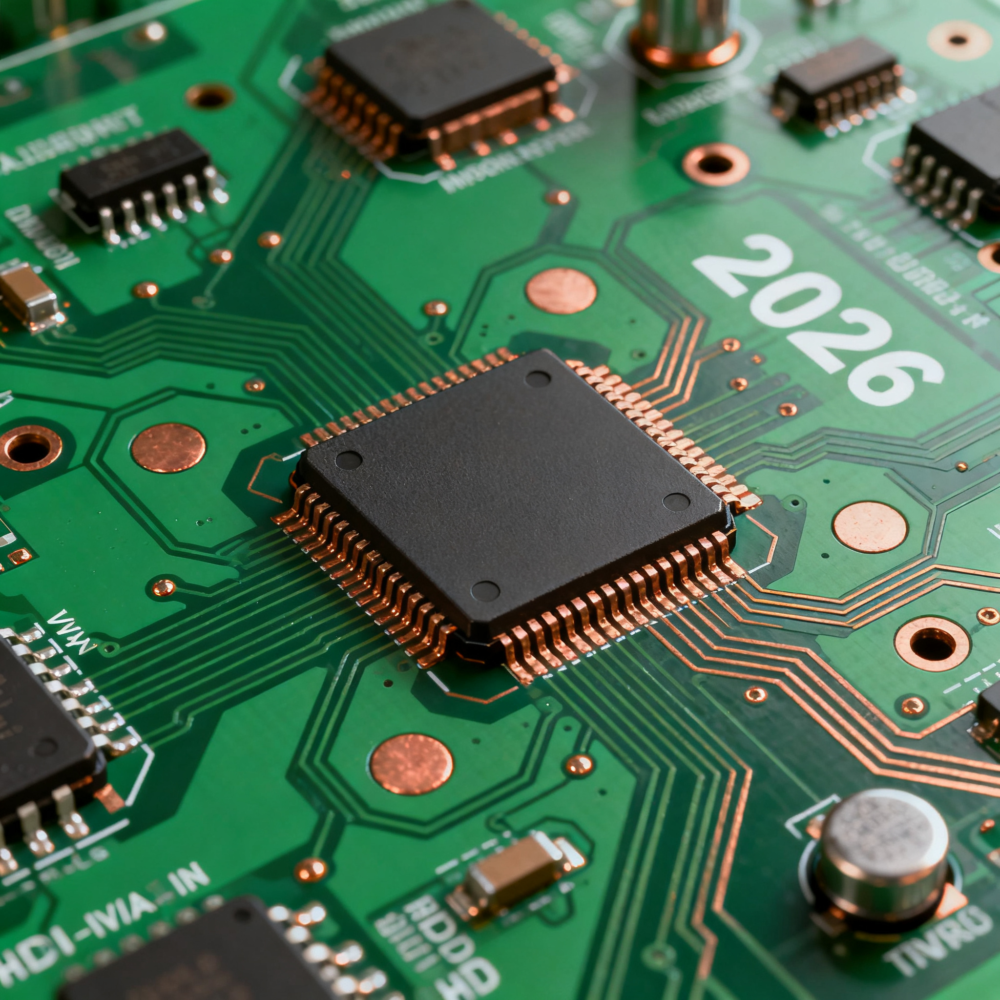
§2 物理/电气/商业底层逻辑深剖 (Root Cause & Mechanistic Analysis)
The core challenges in HDI PCB design, particularly via-in-pad and impedance control, are rooted in fundamental physical and electrical principles. At the heart of these challenges is the need to balance mechanical and electrical integrity while optimizing manufacturing processes.
From a mechanical perspective, via-in-pad technology, which places microvias directly beneath component pads, is critical for achieving high-density layouts. However, this approach requires filled and capped vias to ensure a flat surface for component attachment. Failure to properly fill these vias can lead to microvia voids, as seen in the HeMeiXin PCB case. These voids compromise the mechanical stability of the PCB, leading to potential fractures or delamination under thermal cycling.
Electrically, impedance control is paramount in HDI designs. Impedance discontinuities can result in signal reflections and EMI, particularly in high-speed applications. According to HDI Circuit Board, impedance control involves balancing resistance, capacitance, and inductance to ensure signal integrity. This requires precise stackup configurations and material selection to maintain consistent impedance values (NetVia Group).
To delve deeper into the technical specifications and process parameters, consider the following tables:
Table B: Technical Specifications and Process Parameters
| Parameter | Value/Range | Unit/Notes |
|---|---|---|
| Trace/Space | 30/30 | μm |
| Microvia Diameter | 80 | μm |
| BGA Pitch | 0.4 | mm |
| Impedance Control | 50/100 | Ω |
| Dielectric Thickness | 0.05–0.1 | mm |
| Adhesion Strength | ≥6 | lb./in. |
| Yield Target | ≥92% | Production Yield |
| Thermal Conductivity | 0.8 | W/mK |
Key Takeaways
The data presented in Table B highlights the critical specifications necessary for successful HDI PCB design. The emphasis on precise trace/space dimensions and microvia diameters is essential for maintaining signal integrity and mechanical stability. Additionally, the dielectric thickness and thermal conductivity values are crucial for managing heat dissipation and ensuring the long-term reliability of the board.
Table C: Application and Compliance Considerations
| Application | Compliance Standard | Notes |
|---|---|---|
| Consumer Electronics | IPC-2221 | General Design Standards |
| Automotive Electronics | ISO 9001 | Quality Management |
| Telecommunications | IPC-6016 | HDI-Specific Performance |
| Aerospace | IPC-A-610 Class 3 | High-Reliability Requirements |
| Medical Devices | ISO 13485 | Medical Device Quality |
| Industrial Control | IEC 61010 | Safety Requirements |
Practical Implications
Table C outlines the compliance standards relevant to various applications of HDI PCBs. Adhering to these standards is crucial not only for regulatory compliance but also for ensuring product reliability and safety. For instance, IPC-2221 serves as a general guide for PCB design, while ISO 9001 is essential for maintaining quality management systems in automotive applications.
§3 实时多维度对比模型 (Real-Time Comparative Metric Matrix)
Table A: Comparative Metric Matrix
| 对比维度 (Metrics) | 方案 A (主流原厂/头部方案) | 方案 B (高品质替代/架构) | 选型决定因素与失效边界 |
|---|---|---|---|
| Trace/Space | 30/30 μm | 25/25 μm | Higher density requires precise manufacturing |
| Microvia Diameter | 80 μm | 70 μm | Smaller vias improve signal integrity |
| Impedance Control | 50/100 Ω | 45/90 Ω | Critical for high-speed applications |
| Lead Time | 6–8 weeks | 4–6 weeks | Shorter lead times for rapid prototyping |
| Cost | Higher | Moderate | Cost trade-offs with performance |
Design Considerations
Table A provides a comparative analysis of two HDI PCB design approaches. The primary differences lie in the trace/space dimensions and microvia diameters, with方案 B offering a higher density option. However, this comes with increased manufacturing complexity. Impedance control remains a critical factor, particularly for high-speed applications where signal integrity is paramount. The choice between方案 A and方案 B depends on the specific application requirements and the acceptable trade-offs between performance, cost, and lead time.
§4 全球行业标准合规与防控设计 (Compliance & Risk Mitigation)
Compliance with industry standards is a cornerstone of risk mitigation in HDI PCB design and manufacturing. Standards such as IPC-2221, ISO 9001, and IPC-A-610 Class 3 provide guidelines that ensure product quality and reliability. For instance, IPC-2221 outlines general design standards for PCBs, while ISO 9001 focuses on quality management systems, which are critical for automotive and aerospace applications.
To quantify risk mitigation, manufacturers should consider implementing a 30–35% electrical derating to enhance reliability. Additionally, maintaining a 3-month buffer stock can mitigate supply chain disruptions. Certificates of Conformance (CoC) and traceable closed-loop sourcing are also essential for reducing the risk of counterfeit components and ensuring long-term reliability.
§5 高阶供应链决策导向 FAQ (Advanced Decision-Oriented FAQ)
- Q: How does supplier compliance audit (ERAI/ISO) mitigate this technical/supply risk before PO release?
- A: Supplier compliance audits, such as those conducted by ERAI and ISO, verify that suppliers adhere to industry standards and quality management systems. This process helps to identify potential risks in the supply chain, ensuring that only qualified suppliers are engaged. By conducting audits before the purchase order (PO) release, companies can reduce the likelihood of receiving substandard or counterfeit components, ultimately protecting their brand reputation and product reliability.
- Q: Why does CoC + traceable closed-loop sourcing reduce long-term failure rate?
- A: Certificates of Conformance (CoC) and traceable closed-loop sourcing ensure that all components used in HDI PCBs are authentic and meet specified quality standards. This traceability allows manufacturers to track each component's origin, reducing the risk of counterfeit parts entering the supply chain. By maintaining a closed-loop system, companies can quickly address any quality issues, leading to a lower long-term failure rate and improved product reliability.
- Q: What are the key factors to consider when selecting between方案 A and方案 B in Table A?
- A: When selecting between方案 A and方案 B, key factors to consider include trace/space dimensions, microvia diameter, impedance control, lead time, and cost.方案 A offers a standardized approach with longer lead times and higher costs, while方案 B provides a higher density option with shorter lead times at a moderate cost. The decision should be based on the specific application requirements and acceptable trade-offs between performance, cost, and manufacturing complexity.
- Q: How can manufacturers ensure consistent impedance control in HDI PCB designs?
- A: Consistent impedance control in HDI PCB designs can be achieved by carefully selecting materials and configuring the stackup. Manufacturers should adhere to industry standards such as IPC-6016 for HDI-specific performance and utilize advanced simulation tools to predict impedance values accurately. Regular testing and validation throughout the production process are also essential to maintain impedance consistency and ensure signal integrity.
- Q: What role does thermal management play in HDI PCB reliability?
- A: Thermal management is crucial for HDI PCB reliability, as the high density of components can lead to significant heat generation. Effective thermal management strategies, such as using thermal vias or appropriate dielectric materials with high thermal conductivity, can help dissipate heat efficiently. This prevents overheating, reduces the risk of thermal cycling-induced failures, and extends the overall lifespan of the PCB.
References & Further Reading
- High Density Interconnect (HDI) PCB Designs: A Complete Engineering Guide — HeMeiXin PCB
- HDI Deconstructed — Cadence
- HDI PCB Design Guidelines for Optimized Manufacturability — Matric
- Navigating the Challenges of High-Density Interconnect (HDI) PCB Design — Circuits Central
- HDI PCB Impedance Control: Design, Manufacturing Guide — HDI Circuit Board
- Definition of HDI PCB: Design & Manufacturing Standard — HDI Circuit Board
- IPC Standards — IPC
- ISO 9001 Quality Management — ISO
- HDI PCBs – High Density Interconnect PCBs — NCAB Group
- HDI PCB Design and Manufacturing: From Basics to Advanced Techniques — PCBSync