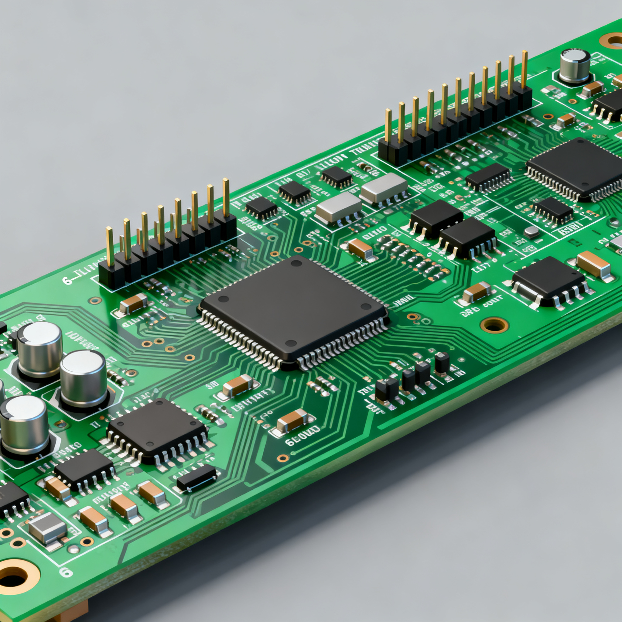
From Tombstoning to Voiding: Real-World Examples of SMT Assembly Defects on 6-Layer High-Density PCBs
Why 6-Layer High-Density PCB Assemblies Amplify Hidden SMT Defects You can design a flawless schematic, source every component on time, and still open a failed assembly report that stops production. T...
Why 6-Layer High-Density PCB Assemblies Amplify Hidden SMT Defects
You can design a flawless schematic, source every component on time, and still open a failed assembly report that stops production. The culprit is often invisible until first-article inspection — a tombstoned 0201 capacitor or a cluster of voids hiding beneath a QFN thermal pad. On 6-layer high-density PCBs, these defects don't just appear more often; they're harder to catch, harder to rework, and more expensive when they escape into the field.
The physics hasn't changed since SMT became the industry standard. What has changed is the density. A modern 6-layer board stacks two or three ground and power planes between tightly packed signal layers, creating thermal masses that pull heat away from small pads at different rates. When the reflow oven can't equalize those temperatures fast enough, the molten solder on one side of a chip component wets and pulls before the other side even reaches liquidus. The result is the classic Manhattan effect: a passive standing upright like a tiny skyscraper.
One real-world failure documented by PCBSync traced tombstoning directly to a design where one pad of an 0402 capacitor necked into a large ground pour without thermal relief. The pour acted as a heat sink, delaying the rise time on that pad by nearly two seconds relative to its neighbor. The solder on the hotter pad melted, wet the termination, and the surface tension torque levered the chip just enough to crack the joint open — not enough to flag at AOI, but enough to fail functional test. That's the maddening reality: on 6-layer boards, tombstoning doesn't always announce itself with a vertical component. Sometimes it leaves a hairline crack that passes electrical test and fails three months later in the customer's enclosure.
Voiding is an even stealthier adversary. Underneath a 7 mm × 7 mm QFN with a solid thermal pad, trapped volatiles from solder paste flux can coalesce into voids that consume 30% or more of the solder joint area. The component still passes ICT because there's enough metallic contact at the pins, but thermal resistance climbs, hotspots form, and reliability degrades silently. Intercole describes voiding as particularly prevalent under bottom-terminated components on multilayer boards, where inner plane copper acts as a heat reservoir that accelerates paste outgassing before solvents can escape. On a 6-layer RF module where every fraction of a decibel matters, a void-ridden thermal pad can shift impedance enough to knock a design out of spec.
These aren't academic concerns. They're daily realities for engineers who push board density to the limit while procurement teams demand first-pass yields above 98%. The next sections break down exactly why these defects occur, how they differ, and what you can do about them before your next prototype spin.
The Physics Behind Tombstoning and Voiding in Dense SMT Stacks
Understanding why a chip component stands up during reflow requires looking at the forces acting on it in the molten state. As solder paste melts, the surface tension of the liquid solder exerts a wetting force on both terminations of the component. If those forces are equal, the component centers itself and settles flat. If one pad reaches liquidus first — or if paste volume differs significantly between the two pads — the resulting torque around the component's center of mass lifts the cooler end. PCBCart refers to this as the Manhattan effect, named for the resemblance to a high-rise building standing on one end.
The mechanism intensifies on 6-layer boards because internal planes create differential thermal paths. A pad tied to a split plane through a narrow thermal spoke heats differently than one connected through a solid web of copper. Even a 0.5-second lag is enough. The smaller the component — 0201 and 01005 passives are the most vulnerable — the lower its thermal mass and the less time it takes for one side to melt ahead of the other.
Voiding operates on a different physical principle. During the preheat and soak phases of reflow, the flux in solder paste volatilizes. Those gases need an escape path. In a standard gull-wing or J-lead joint, the exposed fillet provides ample venting. But under a QFN, BGA, or LGA — components with large bottom-terminated pads — the gases are trapped. If the reflow profile ramps too quickly through soak, the flux volatilizes explosively, bubbles form, and when the solder solidifies, those bubbles remain as voids. ACE Electronics catalogs solder voids alongside bridging and cold joints as one of the most persistent defect categories in modern SMT lines.
On 6-layer boards, the additional copper planes beneath the component slow cooling after peak reflow. That extended liquidus time allows small voids to coalesce into larger ones — a process called Ostwald ripening applied to gas bubbles in molten metal. What starts as fine porosity at 220°C can become a single large void by the time the board exits the cooling zone.
The table below contrasts the four defect types most sensitive to layer-count increases, showing their root causes, how layer count amplifies them, and the detection methods that catch them.
| Defect Type | Root Cause | Layer-Count Sensitivity | Initial Detection Method |
|---|---|---|---|
| Tombstoning | Unequal wetting force from thermal imbalance or paste volume mismatch | High — internal planes create pad-level ΔT of 2–8°C during ramp | AOI with grazing-angle camera |
| Solder Voiding | Flux volatiles trapped under bottom-terminated pads | High — thicker stackups retain heat, extending liquidus time for coalescence | X-ray (2D or CT) |
| Solder Bridging | Excess paste or incorrect stencil aperture dimensions | Medium — finer pitches common on dense boards reduce margin | AOI, post-reflow visual |
| Cold Solder Joints | Insufficient peak temperature or uneven heating across the assembly | High — ground plane heat sinks require profile adjustments | AOI, intermittent electrical test failures |
Notice the pattern: every defect in the table becomes harder to manage as layer count increases. Tombstoning and voiding top the list because their underlying mechanisms — thermal imbalance and gas entrapment — are amplified by the very architecture that makes 6-layer boards attractive for high-density designs. Bridging and cold joints are not far behind; they simply have more established process controls in most factories.
Tip: If your assembly partner runs the same reflow profile for 2-layer and 6-layer versions of the same design, push back. The additional thermal mass of internal planes demands a re-qualified profile with thermocouples placed on the components most susceptible to these four failure modes.
Tombstoning vs. Voiding: Contrasting Failure Modes on High-Layer-Count Boards
Tombstoning and voiding represent opposite ends of the defect spectrum. One announces itself through visible component displacement; the other hides under the component body and degrades performance without any outward sign. Yet both trace their origins to decisions made long before the first PCB panel enters the reflow oven — in pad geometry, layer stackup, stencil aperture design, and thermal profile development.
The table below isolates the contrasts that matter most when you're diagnosing root cause on a failed 6-layer board. Understanding these differences helps you direct your inspection resources correctly: you won't find voids with AOI, and you won't characterize tombstoning torque with X-ray.
| Comparison Metric | Tombstoning (Manhattan Effect) | Solder Voiding | Selection Criteria & Failure Boundary |
|---|---|---|---|
| Primary Origin | Pad thermal imbalance or paste volume asymmetry | Flux outgassing trapped under bottom-terminated components | If defect rate spikes after stackup change, suspect tombstoning; if it rises after paste lot change or profile adjustment, investigate voiding |
| Visual Manifestation | Component lifted on one end, often fully vertical | Internal bubble clusters in solder joint, invisible externally | Use AOI for tombstoning screening; reserve X-ray for voiding assessment |
| 6-Layer Aggravating Factors | Ground plane copper draws heat asymmetrically; pad connected directly to pour without thermal relief | Thicker thermal mass extends liquidus duration; inner plane vias act as gas traps | Board designs with split planes and irregular copper fills are high-risk for both |
| Inspection Technique | AOI with ≥15° angled camera; manual microscope for borderline cases | 2D X-ray; 3D CT for QFN/BGA void location mapping | Inline X-ray catches process drift early; AOI cannot detect voids |
| Rework Feasibility | Possible if caught pre-functional test; component removal and re-soldering required | Impractical — voids embedded in joint cannot be repaired; board-level scrap or concession | Tombstoning rework cost ~$0.50–$2.00 per incident; voiding-related scrap is total loss |
| Prevention Leverage | High — pad geometry, thermal relief design, paste stencil balance | Medium — stencil segmentation, profile soak optimization, via capping under pads | Design-stage decisions yield 80%+ reduction in both defect types |
The rework contrast is especially stark. A tombstoned 0402 resistor is a nuisance: remove it, clean the pads, place a new component, reflow, and move on. A QFN with 35% voiding in its thermal pad is, for all practical purposes, a scrapped board. You can't reflow it again to drive the voids out — reflow profiles are optimized for assembly, not void removal — and the reliability risk of leaving it in place is unacceptable for most end markets. This asymmetry means that voiding prevention deserves proportionally more engineering attention upstream, even though tombstoning is the defect your AOI system flags more visibly.
Greg Smith's analysis at Electronics.org frames the issue through stencil design root cause analysis, showing that "universal" defects — poor paste release, solder balls, bridging, insufficient solder, and voiding — share common origins in aperture geometry and release characteristics. His framework applies directly to 6-layer designs, where the margin for stencil error shrinks as component pitch tightens. Intercole reinforces this from the assembly side, highlighting that PCB warpage during reflow on multilayer boards can compound both tombstoning and voiding by introducing unpredictable standoff variations that alter paste compression and gas escape paths.
Design and Process Rules That Stop SMT Defects Before Reflow
The most effective fix for tombstoning and voiding on 6-layer boards isn't a tighter reflow profile or a more expensive inspection system — it's a set of design and stencil rules applied before Gerber files leave your CAD tool. The patterns are well-documented, and yet they're skipped on a surprising percentage of high-density designs simply because nobody owns the interface between layout and assembly process engineering.
Here are the rules that, applied consistently, eliminate the large majority of these defects:
- Balance copper on small passive pads. When you route a trace from one pad of an 0201 or 0402 directly into a ground pour while the other pad connects through a 6-mil trace to a signal via, you've created a thermal asymmetry. Use thermal relief spokes on both pads, and keep the trace widths matched within 25%.
- Never connect one pad directly to a large copper plane without thermal relief. The PCBSync case study illustrates the failure mode clearly. A solid connection on one side turns that pad into a heat sink. Even with a balanced profile, the temperature delta during ramp can exceed 5°C — enough to trigger tombstoning on 01005 components.
- Optimize stencil aperture area ratio for fine-pitch components. For apertures below a 0.66 area ratio (aperture area divided by wall area), paste release becomes erratic. On 0.4 mm-pitch QFNs and 0201 discretes, this often means specifying electroformed or nano-coated stencils that improve release at small dimensions. Electronics.org provides aperture design guidelines that directly address release consistency.
- Segment thermal pad stencil apertures into window-pane patterns. Instead of one large rectangular aperture for a QFN thermal pad, use a grid of smaller square openings separated by thin webs of unopened stencil. This creates escape channels for flux volatiles during reflow, dramatically reducing voiding percentages without compromising solder joint mechanical strength. DX Circuit identifies this as one of the five most impactful process controls in their 10-step SMT workflow.
- Plug or cap vias under thermal pads. Open vias in the thermal pad area wick solder away from the joint, creating voids and starving the connection. Via-in-pad designs on 6-layer boards should specify conductive fill or at minimum solder-mask-capped vias on the surface layer. This is non-negotiable for QFNs and LGAs with exposed pads.
- Extend the soak zone when profiling for 6-layer assemblies. Where a 2-layer board might use a 60–90 second soak at 150–170°C, a 6-layer board with heavy internal planes often benefits from 90–120 seconds. The extended soak equalizes temperature across the assembly before the ramp to peak, reducing the ΔT that drives tombstoning. NovaPCBA's assembly guide documents this adjustment alongside practical process window parameters.
- Specify thermocouple placement on tomb-prone and void-prone components during profiling. A profile board with thermocouples only on large BGAs tells you nothing about conditions at the 0201 capacitors along the board edge. Attach thermocouples to the specific component locations that history has identified as high-risk.
- Avoid asymmetric copper fills in the inner layers beneath small passives. Even if the outer-layer pads are balanced, a large copper shape on layer 3 beneath only one pad can create a thermal bias that propagates through the dielectric during reflow. Symmetry across all layers is the safest policy.
The table below summarizes key stencil and process parameters with their recommended ranges for 6-layer high-density assemblies, so you can cross-check them against your current setup.
| Parameter | Recommended Value for 6-Layer HDI | Failure Risk Outside Range |
|---|---|---|
| Stencil thickness | 100–120 µm (4–5 mil) | <100 µm: insufficient solder volume for QFN thermal pads |
| Aperture area ratio (smallest) | ≥0.66 | Paste release inconsistency, bridging, insufficient solder |
| Thermal pad aperture segmentation | Window-pane with 50–60% total coverage | Solid aperture: >25% void rate typical; segmented: <10% achievable |
| Soak zone duration (150–170°C) | 90–120 seconds for 6-layer | <60 sec: uneven heating, tombstoning risk; >150 sec: flux exhaustion, oxidation |
| Peak reflow temperature (SAC305) | 235–245°C | <230°C: cold joints on ground-connected pads; >250°C: component damage risk |
| Time above liquidus (TAL) | 60–90 seconds | <45 sec: incomplete wetting; >120 sec: excessive IMC growth, void coalescence |
| Cooling rate | 2–4°C/second | <1°C/s: large grain structure, reduced joint strength; >6°C/s: thermal shock on MLCCs |
| Via treatment under thermal pads | Filled and capped (IPC-4761 Type VII) | Open vias: solder wicking, void formation, joint starvation |
These numbers aren't theoretical. They're pulled from production data across multiple assembly houses and validated by the root cause investigations documented in the sources cited throughout this article. If your current process operates outside any of these windows, you have a systematic defect risk — even if your yields look acceptable today. Process margins erode first at the extremes of component density and layer count.
Questions PCB Engineers and Buyers Ask About SMT Defects on 6-Layer Boards
The following questions come directly from line engineers and procurement leads who've contacted us about 6-layer assembly issues over the past year. Each answer references the material covered in the preceding sections and provides actionable guidance.
Q: Why do 6-layer boards see more tombstoning than 2-layer designs?
The answer lies in thermal mass distribution. Internal ground and power planes in a 6-layer stack act as substantial heat sinks that pull thermal energy away from surface pads at different rates depending on how each pad connects to those planes. A pad connected directly to a ground pour through a thick trace or solid copper shape may lag its counterpart by several degrees during the reflow ramp. That temperature delta translates to one side of a small passive reaching liquidus first, creating a surface tension torque that lifts the cooler end. Two-layer boards, by contrast, have far less buried copper, so the thermal environment across a component's two pads is inherently more symmetric. The fix is copper balancing and thermal relief on both pads — a design rule that's simple to state but frequently overlooked when layout engineers rush to completion. PCBSync's case study shows this exact failure on a production board.
Q: What voiding percentage is acceptable for QFN thermal pads on high-density PCBs?
IPC Class 2 criteria permit up to 25% total void area in the thermal pad solder joint, but many high-reliability customers — particularly in automotive, aerospace, and medical device manufacturing — now specify a maximum of 15%. Above 30% void area, thermal resistance rises sharply, and the resulting hotspots on power components can reduce MTBF by a factor of two or more. For RF applications, voiding above 20% can introduce measurable impedance shifts at frequencies above 2 GHz. The practical takeaway: if your design pushes thermal or RF margins, target single-digit void percentages and use X-ray verification on first-article builds. Intercole provides context on how voiding manifests specifically under bottom-terminated SMT components on multilayer assemblies.
Q: Can we inspect for tombstoning and voiding without X-ray?
Tombstoning — yes. Standard automated optical inspection systems detect lifted components reliably, especially when equipped with grazing-angle cameras that can identify borderline cases where the component has lifted only 25–50 µm. These partial lifts are the most dangerous because they may pass electrical test initially and fail later under thermal cycling. Voiding — no. X-ray inspection is required to see inside the solder joint under BGAs, QFNs, and LGAs. 2D X-ray provides adequate void percentage measurement for most applications; 3D CT adds layer-by-layer void mapping that helps distinguish process-related voiding (bubbles at the component-to-solder interface) from design-related voiding (bubbles around via exits). Inline X-ray systems can now catch voiding trends before entire batches are affected, making them viable for medium-to-high-volume production. ACE Electronics emphasizes that X-ray remains essential for void detection in their defect prevention guide.
Q: How does stencil design influence both tombstoning and voiding simultaneously?
Stencil aperture geometry controls the volume and placement of solder paste deposited on each pad, directly affecting both defect mechanisms. For tombstoning, unequal aperture sizes on the two pads of a chip component starve one side of paste, reducing the wetting force on that termination and allowing the opposite side to lever the component upward during reflow. Even a 10% aperture area difference between the two pads measurably increases tombstoning rates. For voiding, the thermal pad aperture design determines whether flux volatiles have an escape path. A single large aperture traps gases under the component body. Segmenting the aperture into a window-pane pattern — multiple smaller squares separated by narrow stencil webs — provides venting channels that allow gases to escape before the solder solidifies. The same stencil design review should address both defect types because the adjustments affect different aperture features. Greg Smith's stencil design analysis shows the quantitative relationship between aperture geometry and defect rates across multiple defect categories.
Q: When we switch to a 6-layer stackup, do we need to adjust reflow profile parameters?
Yes. More copper layers and denser component populations increase the assembly's overall thermal mass and create larger temperature gradients during ramp and soak. In practice, 6-layer boards typically need a longer soak zone — 90 to 120 seconds versus 60 to 90 seconds for 2-layer equivalents — to equalize temperatures across the assembly before the spike to peak. Peak temperature may also need a 5–10°C boost if large ground planes on inner layers are sinking heat away from surface components. The only reliable way to determine the correct profile is a profile board with thermocouples mounted on the components most susceptible to tombstoning (typically 0201/0402 passives near board edges or large copper pours) and those most prone to voiding (QFN thermal pads and BGA arrays). Running the same profile across all stackup variants without re-qualification is a common source of first-article failures. DX Circuit outlines profile optimization as a distinct step in their assembly workflow, with specific attention to thermal mass differences across board designs.
References & Further Reading
- SMT Defects: Causes and Prevention Guide — ACE Electronics
- Common SMT Defects and How to Avoid Them — PCBCart
- Common SMT Assembly Defects And Their Causes — Intercole
- Solder Joint Defects: 25 Common SMT Defects, Causes & Fixes — PCBSync
- Streamlining SMT Assembly: A Practical Guide — NovaPCBA
- Improve SMT Assembly Yields Using Root Cause Analysis in Stencil Design — Electronics.org (Greg Smith)
- 10-Step SMT Assembly Process (2026): Full PCBA Flow & IPC Class 3 Quality Gates — DX Circuit
- NovaPCBA — Turnkey PCB Assembly Services
The patterns behind tombstoning and voiding on 6-layer high-density PCBs are well-characterized, and the countermeasures are proven. What separates high-yield production from chronic rework isn't knowledge — it's whether design rules are enforced before layout is frozen and whether reflow profiles are re-qualified for the specific thermal mass of each new stackup. NovaPCBA's assembly engineering team reviews every 6-layer and HDI design for these exact defect risks before production release, applying the thermal relief, stencil segmentation, and profile optimization rules detailed above. If you're preparing Gerber files for a 6-layer build and want a manufacturability assessment that catches tombstoning and voiding risks before they become yield losses, our front-end engineering team can run a design review against the parameters documented in this article.