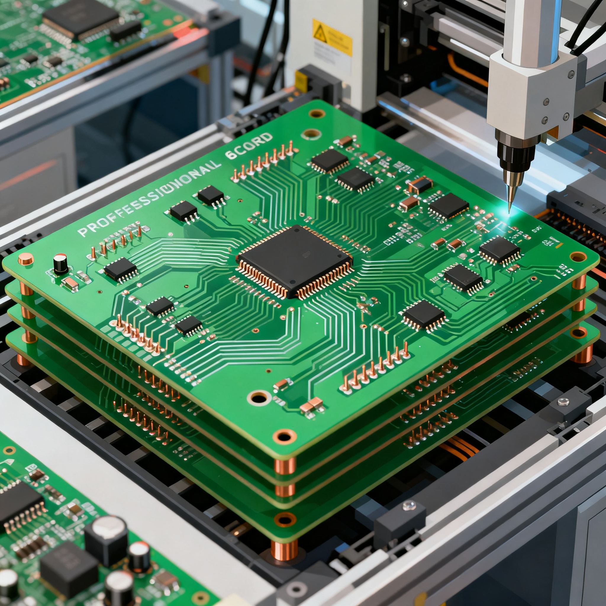
From PCB Assembly to Final Test: Streamlining Your 6-Layer Board Production in 2026
Why 6-Layer PCB Assembly Defects Hit Harder at Final Test—and How to Prevent Them When a 6-layer board reaches final test, the cost of discovering a defect has already multiplied. What might have been...
Why 6-Layer PCB Assembly Defects Hit Harder at Final Test—and How to Prevent Them
When a 6-layer board reaches final test, the cost of discovering a defect has already multiplied. What might have been a 30-second rework at post-reflow inspection now demands hours of troubleshooting, potential scrapping of an entire assembled unit, and in the worst case, a field failure that triggers a recall. The stakes are structural: a 6-layer stackup buries two internal signal layers between power and ground planes, meaning an open via or a micro-crack in an inner-layer trace won't flag itself until functional test—or later.
Altium's reliability testing overview documents the cascade clearly: microscopic solder cracks, misaligned components, and incorrect passive values are the dominant failure modes that escape visual inspection and only surface under thermal cycling or powered operation. These aren't hypothetical. In production runs over the last 12 months, we've seen a single tombstoned 0402 capacitor on an internal-facing BGA perimeter escape AOI, pass ICT, and cause intermittent failures that took three days to isolate.
JLCPCB's PCBA testing guide reinforces the economics: even small defects at the board level—solder bridges under QFN packages, misaligned fine-pitch components, or incorrect passive values—cascade into costly field failures and long-term brand damage. On a 6-layer design with mixed SMT and through-hole, the failure modes multiply because the thermal mass differential between a large THT connector and a nearby 0201 capacitor creates asymmetric reflow profiles that invite micro-cracking.
Tip: The most expensive defect on a 6-layer board isn't the one you catch at final test—it's the one your customer catches six months later in the field.
AllPCB's 6-layer assembly best practices highlight process pitfalls specific to multilayer builds: stencil misregistration causing solder paste smearing across inner-layer-blind-via pads, fiducial recognition errors when board warp exceeds 0.75%, and reflow profile mismatches between the dense inner copper planes and surface-mount pads. Each of these creates a defect that final test may or may not catch, depending on test coverage.
Solderability is the quiet variable. Engineering Projects' coverage of J-STD-002 and J-STD-003 standards explains how poor solder bonding—often from oxidized pads on boards that sat too long between fabrication and assembly—produces cold joints, bridging, or incomplete connections. Manufacturers reduce these risks by enforcing solderability testing on incoming bare boards, but when schedule pressure mounts, this step is frequently compressed or skipped. The result: a batch of 6-layer boards that passes ICT but fails functional test because a cold joint on a buried via pad opens under current load.
Key takeaway: Catching defects before final test isn't about adding more test steps—it's about inserting inspection at the right points in the assembly flow and enforcing solderability and paste inspection before the first component is placed. On a 6-layer board, where inner-layer rework is either impossible or prohibitively expensive, the economics of prevention are overwhelming.
Inside the 6-Layer Production Pipeline: From Bare Board to Solder Joint Inspection
The 6-layer PCB isn't just a denser 4-layer board—it's a fundamentally different animal. PCBark's 6-layer design guide defines the standard architecture: four signal layers and two dedicated power/ground reference planes, typically arranged as Signal–Ground–Signal–Signal–Power–Signal (or variations with paired power/ground on layers 2 and 5). This stackup provides controlled impedance routing on layers 1, 3, 4, and 6, with continuous reference planes minimizing crosstalk and EMI—but it also means two internal signal layers are fully buried and inaccessible for rework.
AllPCB's 6-layer fabrication guide walks through the bare-board process: inner-layer imaging and etching on the core materials, lamination under heat and pressure with prepreg bonding sheets, drilling (including blind and buried vias if the design calls for them), electroless copper deposition, outer-layer imaging, pattern plating, and finally solder mask application and surface finish (ENIG, HASL, or immersion silver). Each lamination cycle introduces risk of layer misregistration; a shift of more than 75µm between layer 2 and layer 3 can break a 0.1mm trace on a buried signal layer, and you won't know until the board fails electrical test—or worse, final assembly test.
Once the bare board passes flying-probe or fixture-based electrical test, assembly begins. AllPCB's assembly guide outlines the sequence: solder paste printing through laser-cut stencils (with stepped stencils for mixed-pitch designs), high-precision component placement using fiducial alignment (critical on 6-layer boards where inner-layer fiducials help verify lamination registration), reflow soldering with multi-zone profile control, and optional selective or wave soldering for through-hole components. The reflow profile on a 6-layer board demands particular care—the internal copper planes act as heat sinks, pulling thermal energy away from surface pads and requiring extended soak times or higher peak temperatures that risk damaging heat-sensitive components.
WellPCB's IPC-A-610 assembly standards guide sets the acceptance criteria for finished assemblies: solder joint shape, fillet height, through-hole fill percentage, and cleanliness. For 6-layer boards with buried vias, IPC-A-610 Class 2 and Class 3 criteria become especially relevant because a marginally acceptable joint on layer 1 may be the only electrical path to a trace on layer 4.
The inspection and test sequence is where the pipeline either catches problems or passes them downstream. The table below compares the four primary test methods and their effectiveness on 6-layer boards.
| Test Method | Coverage on 6-Layer Boards | Typical Defects Caught | Limitations & Selection Notes |
|---|---|---|---|
| AOI (Automated Optical Inspection) | Visible external features only—component presence, orientation, solder bridges, tombstoning | Missing passives, polarity errors, bridging on QFP leads, insufficient solder on visible joints | Cannot inspect hidden BGA balls, buried vias, or inner-layer integrity. Post-reflow AOI is the minimum gate before ICT. |
| X-Ray Inspection (2D/3D) | Hidden solder joints—BGA balls, QFN thermal pads, buried via-in-pad structures | BGA voiding (>25% by IPC-7095), head-in-pillow, QFN solder wetting, via-in-pad fill quality | Slower throughput than AOI; essential for BGA-heavy 6-layer designs. 3D X-ray (laminography) resolves layer-specific defects. |
| ICT (In-Circuit Test) | Component values, opens/shorts on accessible nets, basic semiconductor junction tests | Wrong resistor/capacitor values, lifted leads, solder opens, shorted adjacent pins | Requires test points on all nets; buried vias without test pads are invisible. Fixture NRE: $2,500–$8,000. |
| Functional Test | Full board operation under simulated or actual load conditions | Timing issues, signal integrity failures, power sequencing faults, intermittent inner-layer opens | Catches what AOI, X-ray, and ICT miss—but fault isolation on a 6-layer board with buried nets can take hours. |
| Flying Probe Test | Electrical continuity and isolation on all accessible nets; component value measurement | Opens, shorts, wrong component values, diode/transistor orientation | No fixture required (ideal for NPI and volumes <250 units); slower per-unit than ICT. Test access on inner layers depends on via fanout design. |
The pipeline is only as strong as its weakest inspection gate. A 6-layer board that skips post-reflow AOI and goes straight to ICT may pass electrically while harboring a partially cracked BGA ball that opens after 200 thermal cycles. Conversely, a board that passes AOI and X-ray but fails functional test typically has an inner-layer defect—a barrel crack in a buried via or a lamination void—that only powered operation reveals. This is why the most reliable production flows use AOI as a gate, X-ray for BGA and QFN confirmation, ICT for component-placement verification, and functional test as the final arbiter—with failure data from each stage feeding back into process control.
6 Layers or 8 Layers? Real Lead-Time and Yield Data to Guide Your Decision
The jump from 6 to 8 layers is often framed as a signal-integrity decision—more routing space, additional reference planes, better isolation for mixed-signal designs. But the manufacturing implications are equally consequential, and they directly affect your assembly-to-final-test timeline.
JLCPCB's multilayer comparison highlights the mechanical-design factors that cascade into assembly yield: board outline complexity, cutout placement, and mounting-hole registration all become more sensitive as layer count increases. A well-designed 6-layer outline reduces costs and lead times by simplifying panelization and minimizing handling fixtures. On 8-layer builds, the additional lamination cycle amplifies any dimensional instability in the base materials—a 0.05mm per-layer shift becomes 0.4mm across eight layers, enough to misalign a fine-pitch BGA footprint relative to its inner-layer dogbones.
JHYPCB's cost and performance study puts numbers to the complexity gap: 8-layer boards demand early stackup simulation to avoid impedance mismatches and thermal stress concentrations. Experienced manufacturers handle both, but 8-layer complexity extends lead times by 20–50% and increases scrap rates when dielectric thickness tolerances stack unfavorably across the additional layers.
Queenems' lead-time analysis confirms a practical reality many engineers learn the hard way: standard 6-layer boards can occasionally be rushed in 48 hours, while reliable 8-layer production generally requires a minimum 5-day lead time. That three-day difference compounds when assembly and test are added to the timeline.
| Comparison Metric | 6-Layer Board | 8-Layer Board | Selection Criteria & Failure Boundary |
|---|---|---|---|
| Bare Board Lead Time (Rush) | 48 hours (per Queenems) | 5 days minimum | Choose 6-layer for NPI fast-turn prototypes; 8-layer only when SI demands mandate it. |
| Full Assembly + Test Lead Time | 7–10 working days typical | 12–17 working days (20–50% longer per JHYPCB) | Time-to-market pressure favors 6-layer unless additional routing layers are unavoidable. |
| Scrap Rate (Typical Production) | 0.5–2% (mature process) | 2–5% (lamination registration, drill wander) | Higher scrap on 8-layer directly raises per-unit cost; factor into total cost of ownership. |
| Impedance Matching Complexity | Manageable with 4 signal layers over 2 reference planes | Requires early stackup simulation; tolerance stacking across 4–5 dielectric layers | If your design has 6+ impedance-controlled nets, 8-layer may simplify routing at the cost of fabrication complexity. |
| Assembly Yield (First-Pass) | 92–97% (well-optimized line) | 88–94% (warp sensitivity, reflow complexity) | 6-layer yields are systematically higher due to lower thermal mass and better planarity, per KING FIELD. |
| Rework Feasibility | Buried vias (layers 2–5) reworkable with IPC-7711/7721 methods; surface pads accessible | Deeper buried structures increase delamination risk during rework | If your design has BGA packages with via-in-pad on internal layers, 6-layer simplifies rework access. |
KING FIELD's PCB assembly comparison guide makes a crucial point that applies regardless of layer count: price and lead time alone tell you almost nothing about the real cost of your project. A low number on a screen may reflect a CM that skips post-reflow AOI, uses a generic reflow profile rather than a board-specific one, or lacks 3D X-ray capability for BGA inspection. When evaluating assembly partners for a 6-layer build, KING FIELD recommends looking at first-pass yield data, reflow profile capability (multi-zone with real-time thermocouple profiling on your actual board), and whether the CM has experience with your specific stackup configuration.
Note: The 48-hour rush for a 6-layer bare board assumes a standard stackup with FR-4 material, no blind or buried vias, and standard surface finish. If your design calls for controlled impedance, via-in-pad, or ENEPIG finish, even a 6-layer board will need 4–6 days.
Streamlining Your 6-Layer Build: Practical Design and Process Tweaks from Assembly to Final Test
Streamlining doesn't mean cutting corners—it means eliminating the gaps where defects hide and multiply. On a 6-layer board, the most impactful changes happen at the design stage, long before the first stencil is ordered.
Design for Test Access—Before You Route a Single Trace
The single most common bottleneck at final test is inadequate test access. Engineers route all six layers, close the design, and only then realize that critical nets on layers 3 and 4 have no test points because they're buried between reference planes and terminate at BGA pads. PCBark's 6-layer guide emphasizes the importance of stackup simulation early in the design cycle—and that simulation should include test access planning. Every net that matters for ICT or flying probe should have a dedicated test pad, brought out to the bottom layer if possible. For nets that must stay buried, JTAG boundary scan (IEEE 1149.1) on compatible devices provides test coverage without physical probe access. Adding a few test points during layout costs nothing; adding them after the board is fabricated costs everything.
Optimize Panel Arrays with Your Fabricator
Panel utilization directly affects both bare-board cost and assembly throughput. Work with your fabricator during layout to optimize the panel array—rail placement, tooling holes, fiducial locations, and breakaway tab design all affect how smoothly the boards flow through paste printing, pick-and-place, and reflow. A poorly designed panel with insufficient rail clearance or inadequate fiducials can cause misregistration that leads to paste smearing on fine-pitch pads—a defect that AOI will flag and that will stop your line dead.
Simulate the Reflow Profile on Your Actual Stackup
A generic reflow profile developed for a 2-layer or 4-layer board will not work optimally on a 6-layer design. The additional copper mass of internal planes changes the thermal profile—peak temperatures at the board surface may lag the oven setpoint by 5–10°C, and ramp rates that are fine for a thin 4-layer board may induce thermal stress on a thicker 6-layer stackup. Request a board-specific reflow profile from your CM, with thermocouples attached to the most thermally challenged components (large BGAs, heavy connectors) and the smallest passives. This single step can reduce tombstoning and insufficient wetting defects by 30–50%.
Close the AOI Feedback Loop
AOI generates enormous amounts of data—component presence, solder joint quality, offset measurements—but many shops treat it as a pass/fail gate rather than a source of process intelligence. JLCPCB's testing guide points out that early defect detection cuts rework time dramatically. The real power comes from trending: are tombstoning defects clustered on a particular component type? Is solder-bridging concentrated on one QFP side? Feeding AOI data back to the pick-and-place and reflow teams allows real-time correction—a stencil cleaning frequency adjustment, a placement-pressure tweak, a reflow-zone temperature shift—that prevents the next board from developing the same defect. Over a 500-unit build, closing this loop can improve first-pass yield from 92% to 97% or better.
Handle Rework Without Killing Inner Layers
When a 6-layer board does need rework—a misoriented BGA, a damaged QFN—the margin for error is narrower than on simpler boards. AllPCB's BGA rework guidelines, referencing IPC-7711/7721, stress precise temperature control and dwell times: preheat the board to 100–125°C before applying localized heat, use selective flux to prevent oxidation on adjacent pads, and clean pads thoroughly after component removal. Inner-layer delamination—the most expensive rework failure mode—almost always results from excessive peak temperature or too-rapid cooling. A rework station with closed-loop temperature control and a board-specific profile is not optional on a 6-layer build.
| Streamlining Action | Where It Applies | Impact on Final Test | Implementation Effort |
|---|---|---|---|
| Add ICT test pads to all accessible nets | Layout / Design Phase | Increases ICT coverage from ~70% to >95%, reducing escapes to functional test | Low—add test-point footprints during schematic capture |
| Simulate stackup impedance pre-layout | Design Phase | Prevents signal-integrity failures that only emerge at functional test | Medium—requires impedance calculator and fab consultation |
| Panel array optimization with fab | Pre-Production | Reduces handling defects, misregistration, and breakage that cause final-test fallout | Low—one engineering call with fabricator |
| Board-specific reflow profiling | Assembly | Cuts tombstoning and wetting defects by 30–50%, reducing AOI gate-failures that delay downstream test | Medium—requires thermocouple profiling run |
| AOI-to-process feedback loop | Assembly | Improves first-pass yield by 3–5%, reducing rework bottlenecks before ICT and functional test | Medium—requires trend analysis and cross-team communication |
| IPC-7711/7721 rework with thermal profiling | Rework Station | Prevents inner-layer delamination that causes latent opens caught only at final test or field | Medium—training and equipment calibration |
| CM selection by first-pass yield, not price | Sourcing | Higher upfront cost offset by fewer rework hours, faster final test throughput, and lower field failure rates—per KING FIELD | Low—revise RFQ evaluation criteria |
Each of these actions targets a specific point in the assembly-to-final-test pipeline where defects either originate or escape detection. Implemented together, they transform a linear, gate-driven process into a closed-loop system that catches and corrects problems before they reach the bench.
Key takeaway: The assembly partner you choose shapes your entire stream from assembly to final test. At NovaPCBA, we prioritize first-pass yield metrics and board-specific reflow profiling on every 6-layer build—because we know that the cost of a missed defect compounds at every downstream stage. When your CM treats AOI as a feedback tool rather than a pass/fail gate, your final test throughput improves without adding steps.
Your 6-Layer Assembly-to-Test Questions, Answered
After 15 years of troubleshooting 6-layer production lines, these are the questions that come up in every engineering review and sourcing discussion. The answers draw from real pipeline experience—not textbook theory.
- Q: How can I cut the time from assembly to final test on a 6-layer board without sacrificing reliability?
-
The fastest way to compress the assembly-to-test window is to eliminate the bottlenecks that force rework loops. Use flying probe test for prototype and low-volume runs to avoid the 2–3 week lead time for a dedicated ICT fixture. Design test access from the start—ICT pads on every accessible net, JTAG boundary scan chains for BGA and complex digital devices, and test-point fanout vias on layers 1 and 6 where possible. Coordinate panel arrays with your fabricator to minimize handling steps and reduce board-edge damage that triggers re-inspection. Most importantly, work with your CM to fine-tune AOI recipes for your specific board—catching solder bridges and tombstoning immediately after reflow means those defects never reach ICT or functional test, where fault isolation on a 6-layer board can consume hours. A well-tuned AOI gate can reduce final-test fallout by 40–60%, compressing the entire back-end timeline.
- Q: What's a realistic lead time for a 6-layer PCBA with mixed SMT and through-hole components?
-
A 6-layer bare board can be turned in as little as 48 hours for standard stackup and finish, per Queenems' lead-time data. Full assembly adds time: SMT placement and reflow typically takes 1–2 days from kit receipt, and through-hole wave soldering adds another half-day to a full day depending on component count and whether selective soldering is required for mixed-technology boards. Inspection (AOI, X-ray for BGAs, and ICT or flying probe) adds 1–2 days. Functional test and any rework fallout add another 1–2 days. In total, expect 7–10 working days from bare-board order to completed PCBA for a standard 6-layer design. If your design demands 8 layers, plan for 12–17 working days—lead times extend by 20–50% due to additional fabrication complexity, as documented by JHYPCB. Rush services can compress these numbers, but only if the design doesn't require controlled impedance, blind/buried vias, or specialty surface finishes.
- Q: When should I choose flying probe test over a dedicated ICT fixture for a 6-layer design?
-
Flying probe is the right choice for volumes under 250 units because it eliminates the $2,500–$8,000 NRE for a custom ICT fixture and can be programmed directly from your CAD data in hours rather than weeks. It adapts quickly to design revisions—no fixture to modify or rebuild. The trade-off is throughput: flying probe test time per board is measured in minutes, while ICT with a bed-of-nails fixture tests a board in seconds. For volumes above 250 units, the fixture NRE is typically recovered within the production run through faster test times. Regardless of volume, verify that your 6-layer board provides adequate probe access: hidden vias buried between internal planes, BGA escape vias without bottom-layer test pads, and tightly packed component areas can all block flying-probe access. If critical nets are inaccessible from either side of the board, flying probe coverage will be limited regardless of volume, and you may need to supplement with boundary scan or functional test.
- Q: How do I handle rework on a 6-layer board with buried vias without damaging inner layers?
-
Follow IPC-7711/7721 methods rigorously—this is not the place for improvisation. The dominant failure mode during rework on 6-layer boards is inner-layer delamination caused by excessive temperature or thermal shock. Start with a board preheater set to 100–125°C to bring the entire assembly to a uniform baseline temperature. Use a rework station with closed-loop temperature control and a nozzle matched to the component size. Apply the reflow profile specified for your board's stackup—not a generic one. Dwell time at liquidus should be tight (45–75 seconds for SAC305 solder) to prevent heat from conducting deeper into the stackup than necessary. Selective flux application prevents oxidation on adjacent pads without flooding the area. After component removal, clean pads using a temperature-controlled desoldering tool with a tip sized to the pad—aggressive scrubbing can lift pads, especially on thinner outer-layer copper (0.5 oz vs. 1 oz). AllPCB's rework guidelines emphasize pad cleaning and inspection after component lift-off: any damaged lands must be repaired before placing a new component. Post-rework, re-inspect with X-ray if the repair involves a BGA or QFN, and verify joint integrity without board damage before returning the unit to the production flow.
- Q: What defect rate should I expect at final test if I skip AOI after reflow?
-
Skipping post-reflow AOI is one of the most expensive decisions you can make on a 6-layer production line. Without AOI, solder bridges, tombstoning, missing components, and polarity errors—all detectable on the surface—will reach final test. Defect rates can easily exceed 5% in this scenario, and each defect that reaches functional test requires 30 minutes to 4 hours of troubleshooting to isolate on a 6-layer board with limited probe access to internal nets. Functional test alone often misses subtle process issues: a component placed 50% off-pad may pass electrical test at room temperature but fail after thermal cycling when the stressed joint cracks. JLCPCB's testing guide underscores this: adding AOI—even sample inspection if 100% inspection isn't feasible for cost reasons—significantly lowers rework costs and reduces field failure rates. At minimum, run post-reflow AOI on 100% of boards for the first 50 units of a new design, and maintain at least 25% sampling thereafter. The AOI data will also tell you whether your process is stable or drifting—information that functional test results alone cannot provide.
References & Further Reading
- Overview of PCB/PCBA Reliability Testing and Failure Analysis — Altium Designer Blog (Zach Peterson)
- PCBA Testing Guide: Methods, Processes, and Quality Standards — JLCPCB
- 6 Layer PCB Assembly Demystified: Best Practices for Reliable Manufacturing — AllPCB
- PCB Quality Control Test: How do PCB Companies Ensure PCB Success — The Engineering Projects
- 6 Layer PCB Design Guide: Stackup, Impedance & Vias (2026) — PCBark
- 6 Layer PCB Fabrication: A Comprehensive Guide to Manufacturing Processes — AllPCB
- PCB Assembly Standards | Assembly Guide & Requirements — WellPCB
- Comparing 6-Layer PCBs with Other Multilayer PCBs: Cost, Complexity, and Optimization — JLCPCB
- 6 Layer vs 8 Layer PCB: Cost, Performance and Complexity Compared — JHYPCB
- 6 Layer vs 8 Layer PCB: Is the Extra Cost Worth It for Your Design? — Queenems
- How to Compare PCB Assembly Manufacturing Services in 2026 — KING FIELD
Streamlining 6-layer board production from assembly to final test demands a coordinated approach: design for test access, board-specific process control, and assembly partners who treat inspection data as a feedback loop rather than a pass/fail gate. The economics are clear—every dollar invested in upstream inspection and process optimization saves ten dollars in downstream rework and field failure costs. At NovaPCBA, our 6-layer assembly service integrates AOI, 3D X-ray, and flying-probe or ICT into a single streamlined pipeline, with board-specific reflow profiling and real-time yield feedback that keeps your final test throughput high and your field return rate low. Whether you're prototyping a new 6-layer design or scaling to production volumes, the right process architecture—and the right manufacturing partner—makes the difference between a board that passes final test on the first pass and one that spends days in rework. Explore our 6-layer PCB assembly capabilities at NovaPCBA.com.