From Concept to Board: A Practical Guide to Custom PCB Fabrication Processes
From Concept to Board: A Practical Guide to Custom PCB Fabrication Processes Introduction In the rapidly evolving field of electronics, the ability to design and fabricate custom printed circuit board...
Introduction
In the rapidly evolving field of electronics, the ability to design and fabricate custom printed circuit boards (PCBs) is crucial for innovation and product development. As devices become more sophisticated and compact, the demand for custom PCBs that meet specific performance criteria and fit unique form factors continues to rise. This article provides a comprehensive guide to the PCB fabrication process, focusing on the selection and integration of integrated circuits (ICs) to ensure robust and efficient design.
Technical Overview
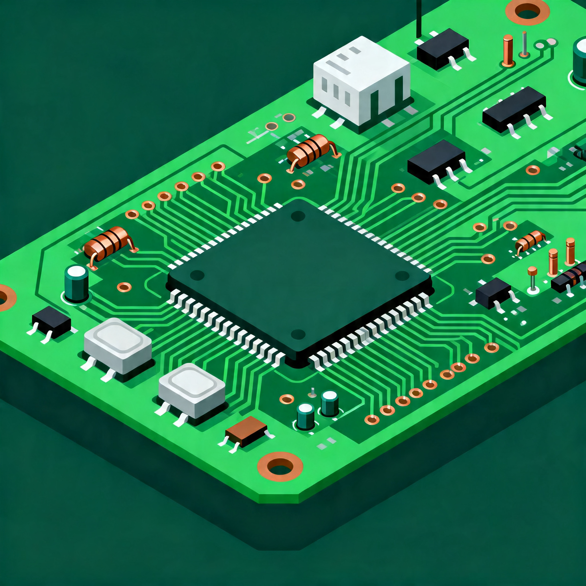
The process of creating a custom PCB involves several critical stages, from initial concept to the final board. Understanding the architecture and principles behind PCB design is essential for ensuring that the final product meets the desired specifications. This includes selecting the appropriate materials, understanding the electrical characteristics, and ensuring compliance with industry standards such as those set by the IPC. The selection of ICs is a pivotal part of this process, as they form the brain of the electronic device, dictating its capabilities and performance.
The architecture of a PCB typically includes layers of conductive material separated by insulating layers. The layout must be carefully designed to support the electrical and thermal requirements of the components. Factors such as trace width, spacing, and via placement play significant roles in the overall performance and reliability of the PCB. Additionally, understanding the thermal and mechanical properties of the PCB material is crucial for ensuring long-term durability.
Detailed Specifications
When selecting an IC for your custom PCB, certain specifications are critical to consider. These include CPU speed, memory capacity, available peripherals, power requirements, and the package type. Each of these factors plays a role in determining the overall performance and compatibility of the IC with your design. The following table outlines some core specifications to keep in mind during the selection process.
| Specification | Details | Importance |
|---|---|---|
| CPU Speed | 1.2 GHz | Determines processing capability |
| Memory | 512 MB RAM, 4 GB Flash | Storage and processing efficiency |
| Peripherals | UART, SPI, I2C | Interface options for external components |
| Power Supply | 3.3V, 500mA | Power efficiency and stability |
| Package | LQFP-64 | Physical size and integration |
| Operating Temperature | -40°C to 85°C | Environmental suitability |
| GPIO Pins | 32 | Flexibility for custom applications |
| ADC Channels | 8 | Analog input capabilities |
| PWM Outputs | 4 | Control for motor and LED applications |
| Security Features | Encryption, Secure Boot | Data protection and integrity |
Key Takeaways from the Specifications
The core specifications outlined in the table highlight the critical aspects to consider when selecting an IC for your PCB. CPU speed and memory are pivotal for determining the processing power and storage capabilities, while available peripherals like UART, SPI, and I2C enable communication with other components. Power supply requirements and package type are essential for ensuring compatibility with your design constraints. Additionally, operating temperature and GPIO availability play significant roles in determining the environmental suitability and flexibility for various applications. By understanding these specifications, you can make informed decisions that align with your design goals.
| Characteristic | Value | Notes |
|---|---|---|
| Supply Voltage | 1.8V to 3.6V | Voltage range for operation |
| Maximum Current | 200 mA | Peak current consumption |
| Input Voltage High | 2.0V (min) | Minimum voltage for logic high |
| Input Voltage Low | 0.8V (max) | Maximum voltage for logic low |
| Output Voltage High | 2.7V (min) | Minimum output voltage for logic high |
| Output Voltage Low | 0.4V (max) | Maximum output voltage for logic low |
| Clock Frequency | 100 MHz | Maximum clock speed |
| Propagation Delay | 5 ns | Delay from input to output |
| Power Dissipation | 500 mW | Heat generated during operation |
| ESD Protection | ±2 kV | Electrostatic discharge protection |
Practical Implications
The electrical characteristics of an IC are crucial for ensuring that it operates efficiently within the desired parameters. Understanding the supply voltage range and maximum current is essential for designing the power supply circuitry. Input and output voltage levels determine compatibility with other digital components, while clock frequency and propagation delay are critical for timing-sensitive applications. Power dissipation must be managed to prevent overheating and ensure long-term reliability. ESD protection is also vital for safeguarding against electrostatic discharge, which can damage sensitive components. These parameters must be carefully considered during the design phase to ensure optimal performance and reliability.
| Application | Configuration | Benefits |
|---|---|---|
| Embedded Systems | Low power, high integration | Efficient for IoT devices |
| Consumer Electronics | High performance, compact | Enhanced user experience |
| Industrial Automation | Robust, reliable | Durability in harsh environments |
| Automotive | High temperature, safety features | Safety and reliability |
| Medical Devices | Precision, low noise | Accuracy and safety |
| Telecommunications | High bandwidth, low latency | Efficient communication |
| Aerospace | Radiation-hardened, lightweight | Performance in extreme conditions |
Application Guidelines
The application comparison table provides insight into how different configurations and specifications can benefit various industries. For embedded systems, low power and high integration are crucial for creating efficient IoT devices. Consumer electronics demand high performance and compact size for an enhanced user experience. Industrial automation requires robust and reliable components to withstand harsh environments. In automotive applications, components must meet high-temperature and safety standards. Medical devices prioritize precision and low noise for accuracy and safety. Telecommunications benefit from high bandwidth and low latency for efficient communication, while aerospace applications require radiation-hardened and lightweight components for performance in extreme conditions. Understanding these configurations and their benefits can guide the selection process for specific applications.
Design Considerations
Designing a custom PCB involves several considerations to ensure functionality and reliability. The layout must accommodate the electrical characteristics of the components, including trace width and spacing to manage impedance and signal integrity. Thermal management is crucial, especially for high-power applications, to prevent overheating and ensure longevity. The choice of materials, such as the substrate and solder mask, can impact the board's performance and durability. Additionally, compliance with IPC standards is essential for quality assurance and reliability. Designers must also consider manufacturability, ensuring that the design can be efficiently produced within budget and time constraints. By addressing these considerations, engineers can optimize their designs for performance and manufacturability.
Signal integrity is another critical aspect, particularly for high-speed applications. Proper termination and routing techniques can minimize signal loss and interference. Power distribution must be carefully planned to ensure stable operation and minimize voltage drops. Component placement and orientation can affect thermal performance and electromagnetic compatibility (EMC). Designers should also consider the potential for future upgrades or modifications, ensuring that the PCB can accommodate changes without significant redesign. By taking a holistic approach to design considerations, engineers can create PCBs that meet both current and future needs.
Step-by-Step Implementation
Implementing a custom PCB design involves several detailed steps, each crucial for ensuring the final product meets the desired specifications and performance criteria. Here is a step-by-step guide to the process:
- Conceptualization: Define the project requirements and specifications. This includes identifying the intended application, performance goals, and any constraints such as size or budget.
- Component Selection: Choose the appropriate components, including ICs, based on the specifications outlined earlier. Consider factors such as availability, cost, and compatibility with other components.
- Schematic Design: Create a detailed schematic diagram that represents the electrical connections and relationships between components. Use design software to ensure accuracy and consistency.
- PCB Layout: Design the physical layout of the PCB, placing components and routing traces to optimize performance and manufacturability. Pay attention to trace width, spacing, and via placement to maintain signal integrity.
- Simulation and Testing: Use simulation tools to test the design for potential issues such as signal integrity, thermal performance, and power distribution. Make necessary adjustments based on the results.
- Prototyping: Manufacture a prototype of the PCB for physical testing. This step allows for real-world evaluation of the design and identification of any issues that may not have been apparent during simulation.
- Testing and Validation: Conduct thorough testing of the prototype to verify that it meets all specifications and performance criteria. This includes functional testing, environmental testing, and compliance with industry standards.
- Finalization and Production: Once the design has been validated, finalize the design for mass production. Work with manufacturing partners, such as PCBWay, to ensure the production process is efficient and meets quality standards.
Common Issues & Solutions
Designing and fabricating a custom PCB can present several challenges. Here are some common issues and their solutions:
- Signal Integrity Problems: High-speed designs may suffer from signal integrity issues, such as reflections and crosstalk. Solutions include using controlled impedance traces, proper termination, and careful routing to minimize interference.
- Thermal Management: Overheating can lead to component failure. Implement heat sinks, thermal vias, and adequate airflow to dissipate heat effectively.
- Power Distribution: Voltage drops and noise in power lines can affect performance. Use decoupling capacitors and proper layout techniques to ensure stable power distribution.
- Component Placement: Poor placement can lead to routing difficulties and performance issues. Use design rules to optimize placement for signal integrity and manufacturability.
- Manufacturing Defects: Issues such as solder bridging and misalignment can occur during production. Work closely with manufacturers to ensure quality control and adherence to design specifications.
Applications & Use Cases
Custom PCBs are used in a wide range of applications, from consumer electronics to industrial systems. In consumer electronics, PCBs enable compact and efficient designs for smartphones, tablets, and wearables. Industrial applications benefit from custom PCBs that provide robust and reliable solutions for automation and control systems. In the automotive industry, PCBs are critical for advanced driver-assistance systems (ADAS) and infotainment systems. Medical devices rely on custom PCBs for precision and reliability in diagnostic and monitoring equipment. Each application presents unique challenges and requirements, highlighting the importance of a tailored approach to PCB design and fabrication.
Selection & Sourcing Guide
Selecting and sourcing the right components for your custom PCB is crucial for ensuring performance and reliability. When choosing components, consider factors such as availability, lead time, and cost. Utilize reliable sources like IC Online to find the components you need. Establish relationships with suppliers to ensure a steady supply of high-quality components. Additionally, consider the potential for component obsolescence and plan for future sourcing needs to avoid disruptions in production.
FAQ
Here are some frequently asked questions regarding custom PCB fabrication:
- What is the typical lead time for PCB fabrication? Lead times can vary depending on the complexity of the design and the manufacturing process. Quick-turn services can deliver within a few days, while standard processes may take several weeks.
- How do I ensure my PCB design meets industry standards? Adhering to IPC standards and conducting thorough testing and validation can ensure compliance with industry standards.
- What are the key considerations for thermal management? Consider the use of heat sinks, thermal vias, and proper airflow to manage heat effectively.
- How can I minimize signal integrity issues? Use controlled impedance traces, proper termination, and careful routing to reduce signal integrity issues.
- What factors influence the cost of PCB fabrication? Factors such as board size, layer count, material choice, and production volume can all influence the cost.
- How do I choose the right components for my PCB? Consider specifications, compatibility, availability, and cost when selecting components.
- What is the importance of ESD protection in PCB design? ESD protection is crucial to prevent damage from electrostatic discharge, which can harm sensitive components.
- How can I ensure reliable power distribution on my PCB? Use decoupling capacitors and a well-planned layout to ensure stable power distribution.
- What are the benefits of using a professional PCB assembly service? Professional services can provide high-quality assembly with fast turnaround times and adherence to quality standards.
- How do I handle component obsolescence? Plan for future sourcing needs and establish relationships with suppliers to ensure a steady supply of components.
Conclusion
Designing and fabricating a custom PCB is a complex process that requires careful consideration of various factors, including component selection, electrical characteristics, and application requirements. By following a structured approach and adhering to industry standards, engineers can create PCBs that meet the desired specifications and performance criteria. This guide provides valuable insights into the process, helping you navigate the challenges and achieve successful outcomes in your PCB projects.