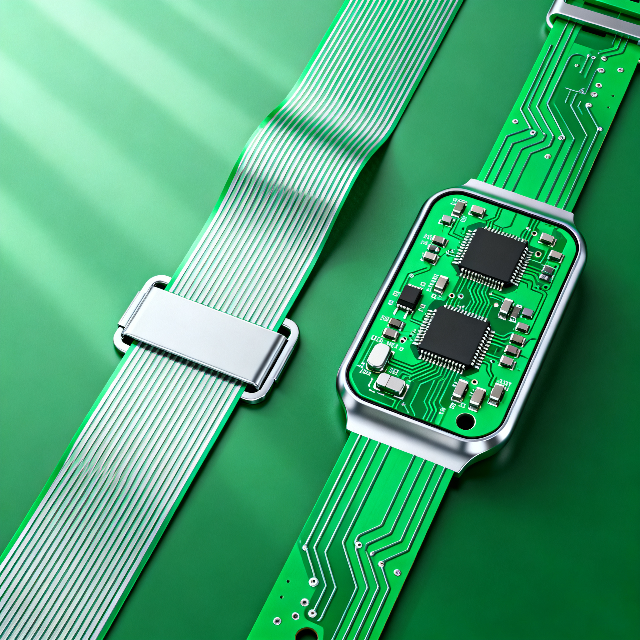
Flex vs. Rigid-Flex PCBA for Wearables: A Selection Guide for Ultra-Thin 2-Layer Designs
When Scaling Wearable Prototypes to Production, the Wrong Board Choice Breaks More Than Budgets You’ve proven your wearable concept on a bench-top prototype. The flex circuit folded perfectly around a...
When Scaling Wearable Prototypes to Production, the Wrong Board Choice Breaks More Than Budgets
You’ve proven your wearable concept on a bench-top prototype. The flex circuit folded perfectly around a wrist mock-up, and the BLE module paired every time. But when you move from five hand-assembled units to a 2,000-piece pilot run, suddenly you’re fighting lifted coverlay, cracked solder joints at the bend zone, and a 12% field failure rate within three months. The root cause isn’t a single bad component—it’s a board architecture that couldn’t survive the transition from prototype to production without process drift.
Maintaining consistency from first article to volume shipment is the single largest challenge in wearable electronics. Leading manufacturers enforce strict material lock-downs, identical soldering profiles, and identical testing protocols across every batch to keep variability below the threshold that triggers field returns (PCBMASTER). A change in polyimide supplier or a 3°C shift in lamination temperature can alter the dynamic bend radius just enough to cause copper fatigue in a smart ring that undergoes 50,000 flex cycles a day.
The stakes are higher in 2025 because wearables have moved beyond simple fitness bands. Medical monitors that track ECG and blood oxygen now require circuits that fold into 3D shapes without connectors, eliminating bulky interposers that add thickness and failure points (KingsunPCB). Smart rings, hearables, and disposable skin patches all demand ultra-thin 2‑layer constructions that can bend, twist, and still maintain signal integrity. Flexible and rigid-flex PCBA solutions are no longer a premium option—they are the only way to meet the mechanical envelope while keeping assembly yields above 95% (PCBSun). This article gives you a practical, no-hype selection guide focused on 2‑layer designs, so you can choose between pure flex with stiffeners and true rigid-flex before you commit to tooling.
What “Ultra-Thin 2‑Layer” Really Means for Flex and Rigid-Flex Stacks
When a wearable spec calls for a 0.2 mm total board thickness, you’re not just squeezing a standard FR-4 stack-up. The core of any ultra-thin 2‑layer design is a polyimide dielectric, typically 0.001–0.002″ (25–50 µm) thick, clad with rolled-annealed copper on both sides (HemeixinPCB). Rolled-annealed copper is essential for dynamic flexing because its elongated grain structure withstands repeated bending far better than electro-deposited copper, which work-hardens and cracks early.
On a pure flex PCB, the copper layers are covered by a polyimide coverlay—a thin film laminated with adhesive—rather than the liquid photoimageable soldermask used on rigid boards. In contrast, rigid-flex constructions add FR‑4 stiffeners only in the component mounting areas, leaving the flex sections bare for folding. The stiffeners are bonded with no-flow prepreg to prevent resin from bleeding into the bend region. Würth Elektronik’s flex design guide notes that flexible soldermask is a varnish-like material that can provide a thinner profile than coverlay in some static applications, but coverlay remains the standard for dynamic wearables (Würth Elektronik Flex Design Guide).
The table below compares the physical characteristics of a typical 2‑layer flex circuit and a 2‑layer rigid-flex stack, both designed for a 0.2 mm total thickness target.
| Parameter | 2‑Layer Pure Flex (with stiffeners) | 2‑Layer Rigid-Flex | Notes |
|---|---|---|---|
| Total thickness (flex area) | 0.12–0.20 mm | 0.15–0.22 mm | Rigid-flex adds thin FR‑4 prepreg layers even in flex zone if not carefully designed. |
| Rigid area thickness | 0.4–0.8 mm (after stiffener lamination) | 0.4–1.0 mm | Stiffeners are bonded with PSA or thermal-set adhesive; rigid-flex uses no-flow prepreg. |
| Minimum static bend radius | ~1.0 mm (5× thickness) | ~1.2 mm (6× thickness) | Rigid-flex transitions demand larger radius to avoid stress at the rigid-flex interface. |
| Minimum dynamic bend radius | ~2.0 mm (10× thickness) | ~2.5 mm (12× thickness) | Dynamic cycling requires conservative radii to achieve 100k+ cycles. |
| Copper type | Rolled-annealed (RA) ½ oz or ⅓ oz | RA in flex layers, ED possible in rigid sections | RA copper mandatory for dynamic flex; ED copper may be used in rigid-only areas. |
| Dielectric material | Adhesiveless polyimide, 25–50 µm | Polyimide core + FR‑4 prepreg in rigid sections | Adhesiveless laminates improve flexibility and Z-axis reliability. |
| Coverlay / Soldermask | Polyimide coverlay (12–25 µm) + adhesive | Coverlay on flex; LPI soldermask on rigid areas | Flex soldermask is possible for static bends but not recommended for dynamic wearables. |
| Component placement | Only on stiffener areas; limited to low-profile passives and small ICs | Full SMT on rigid sections; BGA, QFN, and connectors supported | Rigid-flex allows high-density placement without additional connectors. |
| Relative cost (prototype, 10 pcs) | $150–$400 | $400–$900 | Rigid-flex NRE includes lamination tooling and more complex routing. |
Assembling these ultra-thin substrates introduces another layer of complexity. A 0.15 mm flex circuit is flimsy; it won’t survive a standard SMT line without support. Manufacturers use dedicated pallets or carrier frames to hold the board flat during printing, placement, and reflow. Würth Elektronik’s SLIM.flex technology, for instance, integrates a temporary carrier that is removed after assembly, enabling processing of substrates as thin as 50 µm (Würth Elektronik). If your contract manufacturer doesn’t have experience with thin-flex pallet fixturing, you’ll see tombstoning, solder bridging, and misaligned components on the first run—regardless of how well the board was designed.
Flex Circuit + Stiffener vs. True Rigid-Flex: A Cost-Reliability Trade-Off for 2‑Layer Wearables
At the architectural level, the decision between a simple 2‑layer flex with polyimide stiffeners and a fully integrated rigid-flex stack is a trade-off between upfront cost and long-term reliability under real-world mechanical stress. Both approaches eliminate the need for board-to-board connectors, but they do it with very different risk profiles.
If your wearable has only a handful of sensors and a single BLE module, and the flex circuit’s primary job is to connect two rigid islands, a 1–2 layer flex with stiffeners is not only cheaper but often more reliable than an FFC/FPC connector solution. The elimination of connector contact resistance and the associated assembly step reduces both BOM cost and potential failure points (FlexiPCB). However, as soon as you need to place a 0.4 mm pitch BGA, a QFN package, or multiple sensors on the same rigid area, pure flex with stiffeners runs out of steam. The stiffener lamination process cannot guarantee the flatness and pad coplanarity required for fine-pitch components. In those cases, true rigid-flex is the only way to ensure electrical stability and high first-pass yield (NextPCB).
Cost is not a single number. KingsunPCB reports that rigid-flex PCBs for wearables range from $5 to $300+ per unit, depending on layer count, panel utilization, and order volume (KingsunPCB). A 2‑layer rigid-flex prototype with two rigid sections might cost $800 for 10 pieces, while the equivalent flex-plus-stiffener version costs $250. At 10,000 units, the rigid-flex unit price can drop below $8, while the flex-plus-stiffener remains around $5, but you must factor in the additional assembly labor and yield loss from handling thin stiffeners.
The decision matrix below captures the key differentiators for 2‑layer wearable designs.
| Decision Factor | 2‑Layer Flex + Stiffeners | 2‑Layer Rigid-Flex | Selection Criterion / Failure Boundary |
|---|---|---|---|
| Dynamic bend cycles (to failure) | 50k–150k (adhesive-based coverlay limits life) | 100k–200k+ (adhesiveless construction, no stiffener interface in bend zone) | Choose rigid-flex if the product must survive >100k cycles over its lifetime; flex+stiffener may delaminate at the stiffener edge under repeated flexing. |
| Component density | Low: 0201 passives, small QFN, sensors; no BGAs | High: 0.4 mm pitch BGA, 01005 passives, multiple ICs per rigid island | If you need a BGA or more than 15 components per rigid area, rigid-flex is mandatory for reliable soldering. |
| Assembly complexity | Medium: requires pallet fixturing, stiffener bonding step | High: needs specialized pallets, controlled lamination, and rigid-flex singulation | Both demand a CM with flex assembly experience; rigid-flex adds 3–5 days to prototype lead time. |
| NRE cost (prototype tooling) | $300–$800 | $800–$2,000 | Flex+stiffener is the low-risk entry for proof-of-concept; rigid-flex NRE is justified when the design is frozen. |
| Scalability to volume | Good up to 5k units; beyond that, manual stiffener attachment erodes margin | Excellent: panel-level lamination and automated singulation keep unit cost low at 10k+ volumes | Rigid-flex becomes more cost-effective above 5,000 units when connector BOM and assembly costs are eliminated (NextPCB). |
| Field reliability (3‑year wearable) | Moderate: stiffener delamination risk if adhesive degrades | High: monolithic construction withstands sweat, temperature cycling, and drops | Medical and hearable applications favor rigid-flex for zero-field-failure targets. |
Tip: If your design has only one rigid section (e.g., a smart ring with all components on a single small PCB and a flex tail for the battery), a pure flex with a local stiffener is almost always the right answer. You avoid the rigid-flex lamination cycle and still get a bendable interconnect. Reserve rigid-flex for designs with two or more rigid islands that must fold into a 3D enclosure.
Designing 2‑Layer Wearable Boards That Survive 100,000 Bends and Tight Spaces
A 2‑layer stack-up can be deceptively simple. The real engineering lies in the bend zone geometry, material selection, and assembly process control. The following rules come from field failures we’ve analyzed and from the collective experience of fabricators who specialize in ultra-thin wearables.
1. Bend radius is non-negotiable. For a 0.2 mm thick flex circuit, the dynamic bend radius must be at least 2.0 mm (10× thickness) to prevent copper fatigue. Static bends can go down to 1.0 mm (5×), but only if the board is never flexed after installation. Always follow IPC‑2223 guidelines and ask your fabricator for dynamic bend test data on the exact stack-up you intend to use. Würth Elektronik’s design guide provides stack-up examples that achieve 100 million cycles at 10× thickness with adhesiveless laminates (Würth Elektronik).
2. Trace routing at the bend zone. Never route a 90° corner inside the dynamic flex area. Use curved traces with radii at least 10× the trace width, and stagger traces on the two layers so they don’t stack directly on top of each other. This prevents I‑beam stiffening and distributes stress. Avoid vias in the bend zone entirely; if you must transition layers, do it in a rigid area.
3. Stiffener placement and transition. The edge of a polyimide stiffener creates a hard point where stress concentrates. Extend the stiffener at least 0.5 mm beyond the last component pad, and use a teardrop or tapered end to avoid a sharp 90° corner. For rigid-flex, the transition from rigid to flex should include a generous radius (≥1.5 mm) and a no‑flow prepreg to keep resin out of the flex area (Würth Elektronik).
4. Material choices for longevity. Adhesiveless polyimide laminates eliminate the acrylic adhesive layer that can crack under thermal cycling. Specify rolled-annealed copper with a minimum elongation of 10%. For coverlay, use a 12.5 µm polyimide film with a 15 µm adhesive, and request pad plating (e.g., ENIG) to prevent the coverlay from lifting off small SMD pads during reflow. KingsunPCB notes that properly designed rigid-flex PCBs can last 5–10+ years under repeated bending conditions (KingsunPCB).
5. Assembly survival. Ultra-thin boards demand low-temperature soldering (e.g., SnBi or SnBiAg alloys) to minimize warpage. Use pallets with vacuum hold-down and dedicated support pins. Foxtronics EMS highlights that rigid-flex boards are built to withstand vibration, bending, and thermal stress, but only if the assembly process respects the glass transition temperature of the adhesive and the Z‑axis expansion of the polyimide (Foxtronics EMS). A common pitfall is over-constraining the rigid-flex outline in the panel, which leads to warpage after singulation. Leave enough clearance in the array to allow the flex sections to relax.
6. Prototype-to-production consistency. Before you release a design to volume, verify that your fabricator has a documented process for maintaining material lot traceability, lamination pressure profiles, and electrical test parameters across every batch. As PCBMASTER emphasizes, strict process control is what prevents the subtle shifts that cause field failures (PCBMASTER). A simple audit question: “Show me the dynamic bend test data from your last three production runs of a similar 2‑layer flex circuit.” If they can’t produce it, you’re gambling with your product’s reputation.
The table below summarizes the critical design parameters and their failure boundaries for 2‑layer wearable flex and rigid-flex circuits.
| Design Parameter | Recommended Value / Range | Failure Mode When Exceeded |
|---|---|---|
| Dynamic bend radius | ≥10× total board thickness | Copper fatigue cracking, open circuits after 20k–50k cycles |
| Trace angle in bend zone | Curved, radius ≥10× trace width; no 90° corners | Stress concentration, trace necking, and eventual fracture |
| Stiffener edge distance to pad | ≥0.5 mm, tapered end | Pad lifting, coverlay delamination at stiffener edge |
| Coverlay adhesive squeeze-out | <0.1 mm into pad area | Solder wicking, poor wetting, tombstoning |
| Rigid-flex transition radius | ≥1.5 mm internal radius | Delamination at rigid-flex interface under thermal shock |
| Copper elongation (RA copper) | ≥10% (preferably 15%) | Brittle fracture in dynamic flexing |
| Adhesive type | Adhesiveless for dynamic; acrylic adhesive acceptable for static only | Adhesive cracking, delamination after thermal cycling |
| Assembly peak reflow temperature | ≤160°C for SnBi; ≤220°C for SAC with careful profiling | Board warpage, coverlay blistering, pad lifting |
When you combine these rules with a fabricator that understands wearable-specific requirements, a 2‑layer design can easily meet the 100,000‑bend lifetime that modern fitness bands and medical patches demand. The difference between a product that survives and one that fails in the field often comes down to a 0.2 mm radius on a stiffener edge or the choice of an adhesiveless laminate.
Flex vs. Rigid-Flex for Wearables: Questions Engineers Ask Before Signing Off
After reviewing dozens of wearable projects, we’ve collected the six questions that senior engineers and procurement leads ask most frequently before they release a 2‑layer flex or rigid-flex design to fabrication.
Q: Can I use a 2‑layer flex PCB with stiffeners instead of rigid-flex for a smart ring?
Yes, if the design has only a few sensors and a BLE module. Flex + polyimide stiffeners can handle the tight bend required to wrap inside a ring form factor, but you must verify the dynamic bend radius against the manufacturer’s capability. For a 0.2 mm thick flex, the dynamic radius should be at least 2.0 mm (10× thickness). If your ring diameter forces a tighter bend, you risk copper fatigue. For higher component density or multiple rigid islands, rigid-flex is safer because it eliminates the stiffener delamination risk at the bend transition.
Q: What’s the minimum bend radius for a 0.2 mm thick 2‑layer flex circuit?
Static bend: approximately 1.0 mm (5× thickness). Dynamic bend: approximately 2.0 mm (10× thickness). These values follow IPC‑2223 guidelines and are based on rolled-annealed copper with adhesiveless polyimide. Always confirm with your fabricator’s test data, because the actual minimum depends on copper weight, coverlay thickness, and the number of layers.
Q: How do I manage controlled impedance on a flexible polyimide substrate?
Use adhesiveless laminates with tight thickness tolerance (±10% or better). Polyimide has a dielectric constant (Dk) around 3.4, lower than FR‑4, so you’ll need wider trace geometries to hit 50 Ω or 90 Ω differential. Work with your fabricator to cross-section impedance coupons on the actual flex stack-up. The Würth Elektronik flex design guide includes stack-up examples for 50 Ω single-ended and 100 Ω differential on 2‑layer flex (Würth Elektronik).
Q: What’s the typical lead time difference between flex and rigid-flex prototypes?
Pure flex prototypes can ship in 5–7 working days. Rigid-flex adds 3–5 days due to the additional lamination and routing of rigid sections. In 2025, supply chain pressures on polyimide materials can extend rigid-flex lead times to 15+ days. Plan your prototyping schedule accordingly and always ask for an up-to-date lead time quote before placing an order.
Q: At what production volume does rigid-flex become more cost-effective than flex plus connectors?
Below 1,000 units, flex + connectors is usually cheaper because you avoid rigid-flex NRE and lamination costs. Above 5,000 units, the elimination of connector BOM cost, connector assembly steps, and the reduction in rework due to connector failures make rigid-flex more economical. The exact crossover point depends on your connector cost and assembly yield, but 5,000 units is a reliable planning threshold (NextPCB).
Q: Can I mix rigid and flex sections on a 2‑layer design without increasing the layer count?
Yes. A 2‑layer rigid-flex stack uses the same two copper layers throughout the entire board. The rigid areas are simply laminated with FR‑4 stiffeners (and no-flow prepreg) on one or both sides. This keeps the layer count low while providing solid mounting platforms for components and connectors. The flex sections remain bare polyimide with coverlay, enabling the 3D folding required in wearables.
If your team is evaluating a 2‑layer wearable design and you need a partner that can handle ultra-thin flex assembly with documented process control, NovaPCBA provides turnkey PCBA services for flex and rigid-flex circuits down to 0.12 mm thickness. Our assembly lines use dedicated thin-board pallets and low-temperature soldering profiles validated for wearable volumes from prototype to 50k+ units. Contact our engineering team to discuss your stack-up and get a design-for-manufacturing review before you finalize the layout.
References & Further Reading
- Rigid-Flex PCBs in Wearables: Advanced Design Challenges and Practical Solutions – PCBMASTER
- Top Flex PCB Applications in 2025: Wearables, Medical & More – JHYPCB
- Rigid-Flex PCB Solutions for Smart Wearable Devices (2026 Guide) – KingsunPCB
Want to discuss your project?
Use the quick bar below or this form—we will route you to an engineer.
Contact us