Fast-Tracking Innovation: A Practical Guide to PCB Prototyping Services for Rapid Development
Fast-Tracking Innovation: A Practical Guide to PCB Prototyping Services for Rapid Development Introduction In today's fast-paced electronics industry, rapid prototyping and development are crucial to ...
Introduction
In today's fast-paced electronics industry, rapid prototyping and development are crucial to staying competitive. Printed Circuit Board (PCB) prototyping services have become essential for engineers looking to fast-track innovation and bring new electronic products to market efficiently. As the backbone of modern electronics, PCBs host the components and connections that enable complex functionalities. Understanding component specifications, selecting the right Integrated Circuit (IC) chips, and leveraging PCB prototyping services are vital steps in ensuring successful product development.
Technical Overview
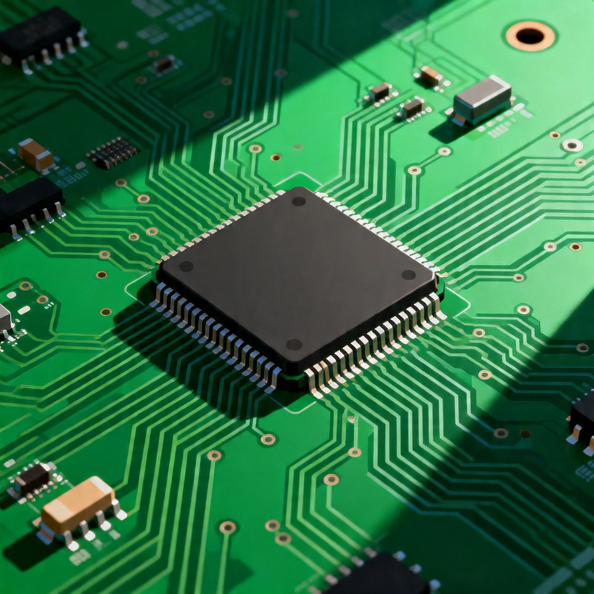
At the heart of any electronic device lies the PCB, a platform that interconnects various components using conductive tracks etched from copper sheets laminated onto a non-conductive substrate. The architecture of a PCB can range from simple single-layer designs to complex multi-layer configurations, each serving different purposes based on the application's needs. The design principles involve optimizing signal integrity, managing thermal performance, and ensuring mechanical robustness. PCB prototyping services play a crucial role in validating these designs by providing quick iterations and testing capabilities. Understanding the core concepts of PCB design, including component placement, routing strategies, and layer stack-up, is fundamental for engineers aiming to harness the full potential of rapid prototyping services.
Detailed Specifications
When selecting IC chips for PCB design, several core specifications need to be considered. These specifications include the CPU speed, memory capacity, available peripherals, power requirements, and packaging options. Each of these factors influences the overall performance, efficiency, and suitability of the IC for specific applications. Understanding these specifications is essential for making informed decisions and ensuring that the chosen components align with the project requirements.
| Specification | Details | Comments |
|---|---|---|
| CPU Speed | 1.2 GHz | Suitable for high-performance applications |
| Memory | 256 MB RAM, 512 MB Flash | Adequate for embedded systems |
| Peripherals | UART, SPI, I2C | Supports diverse communication protocols |
| Power Supply | 3.3V | Common voltage level for low-power designs |
| Package Type | QFN-32 | Compact and easy to mount |
| Operating Temperature | -40°C to 85°C | Wide range suitable for industrial applications |
| GPIO Pins | 20 | Flexible for various input/output configurations |
| ADC Channels | 8 | Supports multiple sensor inputs |
| PWM Outputs | 4 | Useful for motor control applications |
| Package Dimensions | 5mm x 5mm | Space-efficient design |
Key Takeaways from the Specifications
The specifications outlined in the table provide a comprehensive overview of the capabilities and limitations of the IC chip under consideration. The CPU speed of 1.2 GHz ensures that the chip can handle demanding tasks, making it ideal for high-performance applications. The memory configuration, with 256 MB RAM and 512 MB Flash, is sufficient for a wide range of embedded systems. The inclusion of multiple peripherals such as UART, SPI, and I2C offers versatility in communication options. The power supply requirement of 3.3V is standard for low-power designs, while the QFN-32 package type offers a compact form factor that is easy to integrate into various PCB layouts. These specifications are critical for evaluating the suitability of the IC chip for specific applications and ensuring alignment with project goals.
| Parameter | Value | Comments |
|---|---|---|
| Operating Voltage | 3.0V - 3.6V | Stable operation within this range |
| Max Current Consumption | 200 mA | Under peak load conditions |
| Input Capacitance | 5 pF | Low input capacitance for fast signal response |
| Output High Voltage | 2.8V min | Ensures strong logic high signal |
| Output Low Voltage | 0.4V max | Maintains clear logic low state |
| Propagation Delay | 5 ns | Fast response time for high-speed applications |
| ESD Protection | 2 kV | Robust protection against electrostatic discharge |
| Leakage Current | 1 µA | Minimal leakage for energy efficiency |
| Clock Frequency | 24 MHz | Supports high-speed clock operations |
| Thermal Resistance | 30°C/W | Effective heat dissipation |
Practical Implications
The electrical characteristics table provides insights into the operational parameters and limitations of the IC chip. The operating voltage range of 3.0V to 3.6V ensures stable performance, while the maximum current consumption of 200 mA indicates the power budget required under peak conditions. The low input capacitance and fast propagation delay highlight the chip's suitability for high-speed applications. ESD protection of 2 kV and minimal leakage current enhance the chip's robustness and energy efficiency. Understanding these electrical characteristics is crucial for optimizing the design for performance and reliability, ensuring that the IC chip will function effectively within the specified operational parameters.
| Application | Configuration | Benefits |
|---|---|---|
| Wearable Devices | Low-power, compact design | Extended battery life, small form factor |
| Industrial Automation | Robust, wide temperature range | Reliable in harsh environments |
| IoT Sensors | Multiple ADC channels | Efficient data acquisition |
| Smart Home Devices | Versatile communication interfaces | Seamless integration with IoT networks |
| Consumer Electronics | High-performance CPU | Enhanced user experience |
| Medical Devices | Low leakage current | Safe and energy-efficient operation |
| Automotive Systems | High ESD protection | Improved safety and reliability |
Application Guidelines
The application comparison table highlights the versatility and adaptability of the IC chip across various use cases. For wearable devices, the low-power and compact design offer extended battery life and a small form factor, crucial for user comfort and practicality. In industrial automation, the chip's robustness and wide operating temperature range ensure reliable performance in demanding environments. IoT sensors benefit from the multiple ADC channels, facilitating efficient data acquisition. Meanwhile, smart home devices leverage versatile communication interfaces for seamless integration with IoT networks. Each application presents unique requirements that the IC chip can meet, demonstrating its broad applicability and effectiveness in diverse scenarios.
Design Considerations
When embarking on PCB design, several key considerations must be addressed to ensure a successful implementation. First, component selection is critical; engineers must choose components that align with the application's performance requirements and environmental conditions. This involves evaluating datasheets and specifications to ensure compatibility and reliability. Signal integrity is another crucial factor, requiring careful routing and layout to minimize interference and maintain clean signal transmission. Thermal management is equally important, necessitating strategies such as heat sinks or thermal vias to dissipate heat effectively and prevent component failure. Additionally, adhering to industry standards, such as those from IPC, ensures that the design meets quality and safety benchmarks. Collaboration with PCB prototyping services can provide valuable feedback and iterations, helping to refine the design and address potential issues before mass production.
Step-by-Step Implementation
Implementing a PCB design involves several critical steps, each requiring careful planning and execution:
- Define Requirements: Establish the functional and performance requirements of the PCB, including size, power, and connectivity needs.
- Select Components: Choose the appropriate IC chips, passive components, and connectors based on the project's specifications.
- Create Schematic: Develop a detailed schematic diagram that outlines the electrical connections and component placements.
- Design PCB Layout: Use CAD software to design the PCB layout, ensuring optimal component placement and routing for signal integrity.
- Prototype Fabrication: Collaborate with a PCB prototyping service to fabricate a prototype for testing and validation.
- Testing and Validation: Conduct thorough testing to verify the PCB's functionality, performance, and compliance with specifications.
- Iterate and Refine: Use feedback from testing to refine the design, addressing any issues or improvements identified.
- Prepare for Production: Finalize the design, generate manufacturing files, and coordinate with a PCB manufacturer for production.
Common Issues & Solutions
During PCB prototyping and development, engineers may encounter several common issues that require prompt solutions:
- Signal Integrity Problems: Use controlled impedance routing and implement proper grounding techniques to minimize signal loss and interference.
- Thermal Management Challenges: Incorporate thermal vias, heat sinks, and appropriate copper thickness to manage heat dissipation effectively.
- Component Placement Conflicts: Optimize component placement to ensure adequate spacing and prevent overlapping or interference.
- Power Supply Instability: Implement decoupling capacitors and voltage regulators to maintain stable power supply levels.
- Manufacturing Defects: Adhere to IPC standards and conduct thorough inspections to identify and rectify defects before production.
- Testing Inaccuracies: Use precise testing equipment and methodologies to ensure accurate and reliable test results.
Applications & Use Cases
PCB prototyping services are utilized across a wide range of applications, from consumer electronics to industrial automation. In wearable technology, PCBs enable the integration of sensors and connectivity features within compact devices. In the automotive industry, PCBs are critical for advanced driver-assistance systems (ADAS) and infotainment systems. The proliferation of IoT devices relies heavily on PCBs for connectivity and data processing. Medical devices use PCBs to ensure precise and reliable operation in life-critical applications. Each use case presents unique challenges and opportunities, highlighting the importance of tailored PCB design and prototyping strategies.
Selection & Sourcing Guide
Selecting and sourcing the right IC chips and components is crucial for successful PCB design and implementation. Engineers should evaluate component specifications, availability, and supplier reliability. Online resources such as IC Online provide valuable information and access to a wide range of components, facilitating informed decision-making and efficient sourcing.
FAQ
- What is the importance of PCB prototyping? PCB prototyping allows engineers to test and validate designs before mass production, reducing the risk of errors and ensuring functionality.
- How do I choose the right IC chip for my project? Evaluate the chip's specifications, such as CPU speed, memory, and peripherals, and ensure they align with your project's requirements.
- What are the benefits of using PCB prototyping services? These services offer quick turnaround times, flexibility in design iterations, and access to advanced manufacturing technologies.
- How can I ensure signal integrity in my PCB design? Use proper routing techniques, controlled impedance, and adequate grounding to minimize interference and signal loss.
- What are the common challenges in PCB design? Challenges include signal integrity, thermal management, component placement, and manufacturing defects.
- How do I test a PCB prototype? Conduct functional testing, performance evaluation, and compliance checks using precise testing equipment and methodologies.
- What standards should I follow for PCB design? Adhere to IPC standards, such as IPC-A-610 and IPC-2221, for quality and safety compliance.
- How do I manage thermal issues in a PCB? Implement thermal vias, heat sinks, and appropriate copper thickness to enhance heat dissipation.
- What is the role of datasheets in component selection? Datasheets provide detailed specifications and operational parameters, guiding engineers in selecting suitable components.
- How can I source components efficiently? Use online platforms like IC Online to access a wide range of components and ensure reliable sourcing.
Conclusion
PCB prototyping services are indispensable tools for engineers seeking to innovate rapidly and efficiently. By understanding component specifications, leveraging advanced prototyping techniques, and adhering to industry standards, engineers can develop robust and reliable electronic products. The insights gained from prototyping and testing pave the way for successful product launches and sustained competitiveness in the ever-evolving electronics industry.