Estimating PCB Prototype Costs: A Detailed Breakdown for Rapid Development Projects
Estimating PCB Prototype Costs Introduction In the competitive landscape of electronics development, rapid prototyping is essential for staying ahead. Printed Circuit Boards (PCBs) are the backbone of...
Introduction
In the competitive landscape of electronics development, rapid prototyping is essential for staying ahead. Printed Circuit Boards (PCBs) are the backbone of most electronic devices, and understanding their prototype costs is crucial for budget management and project planning. This article delves into the intricate details of estimating PCB prototype costs, focusing on component specifications, selection criteria, and application circuits. Understanding these factors can significantly impact the efficiency and cost-effectiveness of your development projects.
Technical Overview
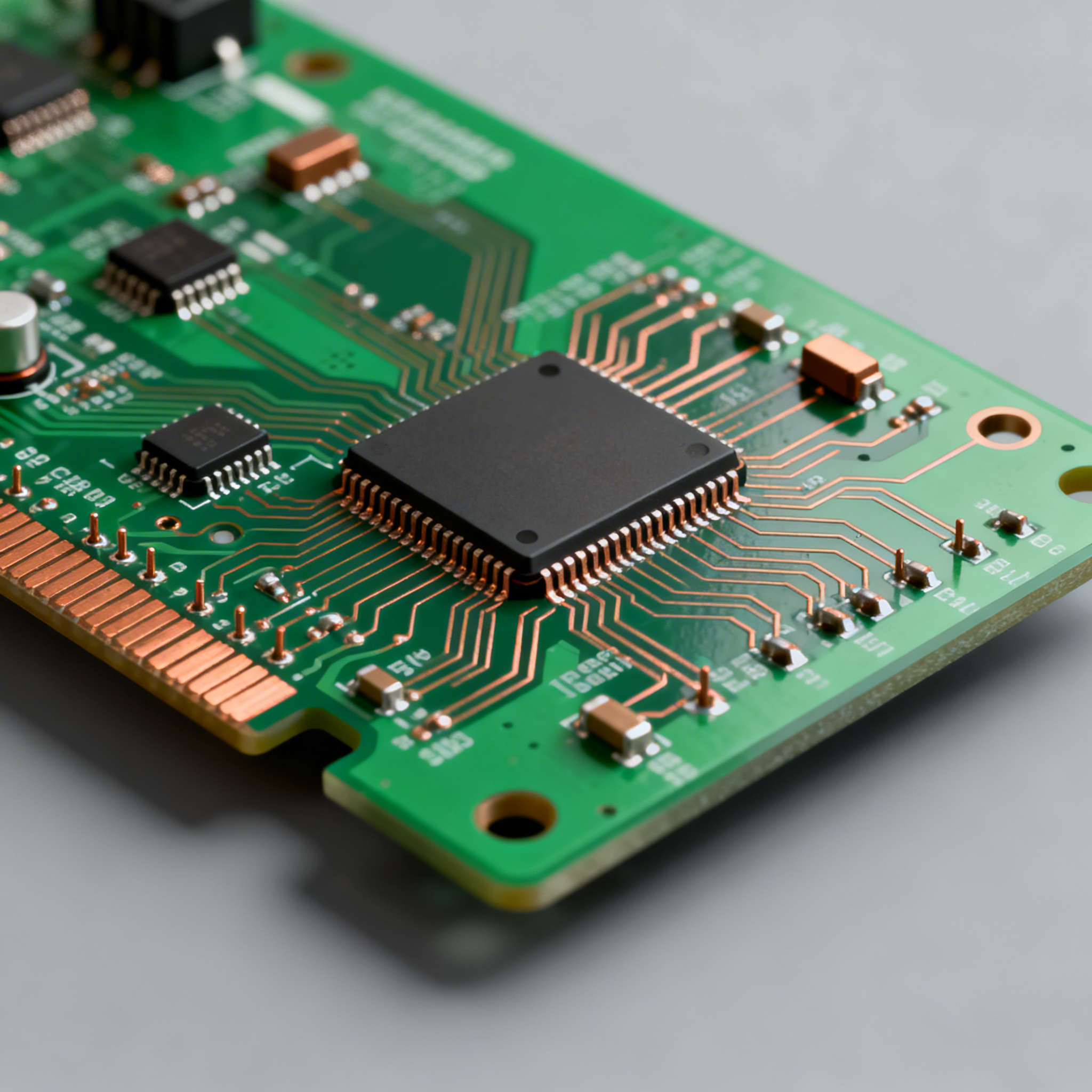
The core of PCB prototyping revolves around design, manufacturing, and assembly. The design phase involves creating a schematic and layout, adhering to IPC standards such as IPC-A-610 for assembly acceptability and IPC-2221 for design standards. Manufacturing translates these designs into physical boards, where factors like layer count, board thickness, and material type play significant roles. Assembly involves placing components onto the board, requiring precision and adherence to specifications. Each step has associated costs, and understanding these can help in accurately estimating the total prototype cost.
Detailed Specifications
Specifications are the fundamental parameters that define a PCB's functionality and performance. Key specifications include board dimensions, layer count, material type, copper thickness, and surface finish. These elements influence not only the cost but also the reliability and longevity of the PCB. Below is a detailed table highlighting the key specifications you should consider during the prototype phase.
| Specification | Parameter | Typical Values |
|---|---|---|
| Board Dimensions | Length x Width | 100mm x 100mm |
| Layer Count | Number of Layers | 2 to 12 |
| Material Type | FR-4, Rogers | FR-4 |
| Copper Thickness | Ounces per Square Foot | 1 oz |
| Surface Finish | HASL, ENIG | HASL |
| Drill Hole Size | Minimum Diameter | 0.3mm |
| Trace Width | Minimum Width | 0.2mm |
| Impedance Control | Required/Not Required | Required |
| Solder Mask Color | Color Options | Green |
| Silkscreen | Color Options | White |
Key Takeaways from the Specifications
The specifications table provides a snapshot of the critical parameters that influence the PCB's cost and performance. For instance, opting for a higher layer count increases complexity and cost but is necessary for advanced circuits. Material type like FR-4 is commonly used due to its balance of performance and cost-effectiveness. Copper thickness and surface finish also impact thermal performance and solderability. Understanding these elements allows for informed decision-making, ensuring the prototype meets both budgetary and technical requirements.
| Metric | Characteristic | Typical Values |
|---|---|---|
| Thermal Conductivity | W/m·K | 0.3 |
| Dielectric Constant | εr | 4.2 |
| Loss Tangent | tan δ | 0.02 |
| Glass Transition Temp | Tg (°C) | 130 |
| Coefficient of Thermal Expansion | ppm/°C | 17 |
| Moisture Absorption | % | 0.1 |
| Surface Resistivity | Ω/sq | 10^6 |
| Volume Resistivity | Ω·cm | 10^8 |
| Peel Strength | lb/in | 7 |
Practical Implications
The performance metrics table highlights critical electrical and thermal characteristics that affect the PCB's functionality. Thermal conductivity and glass transition temperature are vital for applications involving high heat. A low dielectric constant is preferable for high-frequency applications to reduce signal loss. Moisture absorption and surface resistivity indicate the board's reliability in different environmental conditions. By evaluating these metrics, designers can predict how the PCB will perform under operational stresses, ensuring it meets the required reliability standards.
| Application | Configuration | Specific Use Cases |
|---|---|---|
| Consumer Electronics | 2-4 Layer | Smartphones, Tablets |
| Automotive | 6-8 Layer | ECUs, Infotainment Systems |
| Industrial Controls | 4-6 Layer | PLC, HMI |
| Telecommunications | 8-12 Layer | Routers, Switches |
| Medical Devices | 4-8 Layer | Diagnostic Equipment |
| Aerospace | 10-12 Layer | Avionics, Satellite Systems |
Application Guidelines
The application matrix provides insights into the typical configurations and use cases for various industry sectors. Consumer electronics often use simpler, cost-effective 2-4 layer boards, while aerospace applications require complex, high-reliability 10-12 layer boards. Understanding the application requirements helps in selecting the appropriate PCB configuration, balancing performance with cost. This knowledge is crucial for optimizing the design to meet specific industry standards and operational demands.
Design Considerations
Designing a PCB requires careful consideration of various factors to ensure optimal performance and cost-effectiveness. Start with a clear understanding of the circuit requirements and design constraints. Utilize design rules provided by manufacturers like PCBWay to avoid common pitfalls. Pay attention to trace width and spacing to prevent signal integrity issues. Consider thermal management, especially for high-power applications, and ensure proper grounding and shielding for noise reduction. Using design software with simulation capabilities can help identify potential issues early in the design process. Collaboration with assembly services like Nova PCBA can provide valuable insights into manufacturability and cost implications.
Step-by-Step Implementation
Implementing a PCB prototype involves several key steps:
- Define Requirements: Outline the electrical and mechanical specifications based on the application.
- Create Schematic: Use CAD software to design the circuit, ensuring all components are correctly placed and connected.
- Design Layout: Translate the schematic into a PCB layout, considering trace routing, layer stacking, and component placement.
- Simulate Design: Conduct electrical and thermal simulations to validate the design and identify potential issues.
- Review and Optimize: Perform design rule checks and optimize for manufacturability and cost.
- Submit for Manufacturing: Send the final design files to a PCB manufacturer for fabrication.
- Assembly and Testing: Assemble the PCB with components and conduct functional testing to ensure it meets specifications.
- Iterate as Needed: Based on test results, make necessary design adjustments and repeat the process if required.
Common Issues & Solutions
PCB prototyping can encounter several common issues, including:
- Signal Integrity Problems: Use proper trace routing and impedance control to minimize signal reflection and crosstalk.
- Thermal Management: Implement heat sinks and thermal vias to dissipate heat effectively.
- Component Placement Errors: Ensure adequate spacing and orientation for components to facilitate assembly and testing.
- Power Distribution Issues: Design robust power planes and decoupling strategies to ensure stable power delivery.
- Solder Joint Reliability: Optimize reflow profiles and use appropriate solder paste to enhance joint quality.
- Manufacturing Defects: Collaborate with experienced manufacturers and use automated inspection techniques to detect defects early.
Applications & Use Cases
PCBs are used across various industries, each with unique requirements. In consumer electronics, PCBs are designed for compactness and cost efficiency. Automotive PCBs must withstand harsh environments and vibration. Industrial controls demand reliability and robustness, while telecommunications require high-speed data handling. Medical devices prioritize safety and precision, and aerospace applications focus on weight and durability. Understanding these use cases helps tailor the PCB design to meet specific industry needs.
Selection & Sourcing Guide
Selecting components for your PCB involves balancing performance, cost, and availability. Utilize resources like IC Online for sourcing components with comprehensive datasheets and availability information. Consider lead times and supplier reliability to ensure timely project completion. Evaluate multiple suppliers to get competitive pricing and ensure quality standards are met.
FAQ
Here are some common questions regarding PCB prototyping:
- What factors most influence PCB cost? Layer count, material type, and board size are significant cost drivers.
- How can I reduce PCB prototype costs? Optimize design for manufacturability, use standard materials, and minimize layer count where possible.
- What is the importance of impedance control? Impedance control is crucial for signal integrity, especially in high-frequency applications.
- How do I ensure PCB reliability? Use quality materials, follow design guidelines, and conduct thorough testing.
- What should I consider when selecting a PCB manufacturer? Look for experience, capability, quality certifications, and customer reviews.
- What is the typical turnaround time for PCB prototyping? Depending on complexity, it can range from a few days to several weeks.
- Why is thermal management important? Proper thermal management prevents overheating, ensuring longevity and reliability.
- How do I choose the right surface finish? Consider factors like solderability, shelf life, and environmental exposure.
- What role does simulation play in PCB design? Simulation helps identify potential issues and validate design decisions early in the process.
- How do I handle design changes during prototyping? Use modular design approaches and maintain clear documentation to manage changes efficiently.
Conclusion
Estimating PCB prototype costs requires a comprehensive understanding of specifications, performance metrics, and application requirements. By carefully considering these factors and leveraging industry resources, engineers can optimize their designs for cost and performance. Whether working on consumer electronics or aerospace applications, a methodical approach to PCB design and prototyping can lead to successful project outcomes.