Essential PCB Testing Methods: Troubleshooting Techniques for Ensuring Quality and Reliability
Essential PCB Testing Methods: Troubleshooting Techniques for Ensuring Quality and Reliability Introduction In the realm of electronics, printed circuit boards (PCBs) are the backbone of virtually eve...
Introduction
In the realm of electronics, printed circuit boards (PCBs) are the backbone of virtually every electronic device. Ensuring the quality and reliability of PCBs is critical, as any flaw can lead to device malfunction, increased costs, and even safety hazards. This article delves into essential PCB testing methods, focusing on the critical aspects of PCB layout rules, stackup design, signal integrity, and manufacturing considerations. By understanding these facets, engineers can troubleshoot effectively and ensure high-quality, reliable PCBs.
Technical Overview
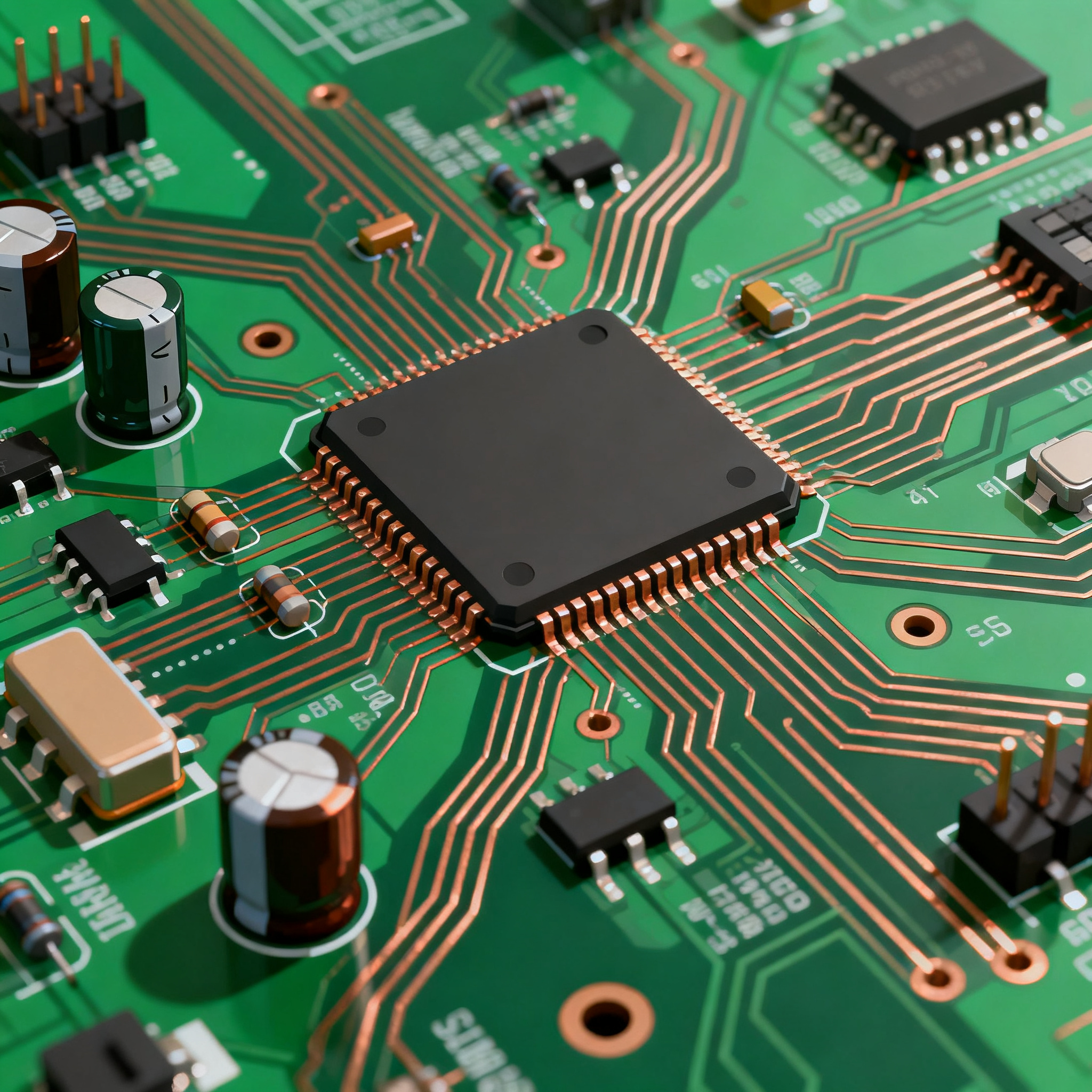
The design and manufacture of PCBs involve a complex interplay of technical principles. At the core, PCBs consist of a substrate material, typically FR-4, with conductive pathways etched from copper sheets. These pathways connect various electronic components, facilitating electrical flow. The architecture of a PCB can range from single-layer to multi-layer, depending on the complexity of the circuit. Signal integrity, a crucial aspect of PCB design, refers to the preservation of the quality of electrical signals. It is influenced by factors such as trace width, spacing, and layer stackup. Manufacturing considerations encompass the selection of materials, adherence to design standards like IPC-A-610 and IPC-2221, and the capabilities of fabrication facilities. Mastery of these concepts is essential for designing PCBs that meet performance specifications and regulatory requirements.
Detailed Specifications
Specifications in PCB design are critical as they dictate the board's performance, reliability, and manufacturability. Key specifications include trace width, spacing, via sizes, and clearances. These elements ensure that the PCB can handle the required current loads without signal loss or interference.
| Design Parameter | Recommended Value | Description |
|---|---|---|
| Trace Width | 0.2 mm | Width of the copper trace to handle specified current |
| Trace Spacing | 0.2 mm | Minimum distance between traces to prevent shorts |
| Via Diameter | 0.6 mm | Diameter of drilled holes for connections between layers |
| Annular Ring | 0.15 mm | Ring of copper around via holes for secure connections |
| Pad Size | 0.8 mm | Area of copper for component soldering |
| Clearance | 0.2 mm | Space between copper features and board edges |
| Layer Count | 2-16 Layers | Number of conductive layers in the PCB |
| Aspect Ratio | 8:1 | Ratio of board thickness to smallest hole diameter |
| Impedance Control | ±10% | Tolerance for characteristic impedance in traces |
| Solder Mask Clearance | 0.1 mm | Gap between solder mask and copper pads |
Key Takeaways from the Specifications
The specifications outlined in the table are critical for ensuring the PCB's functionality and reliability. For instance, trace width and spacing are designed to handle specific current loads and prevent signal interference. The via diameter and annular ring ensure secure electrical connections between layers, while the pad size and clearance are crucial for component soldering and preventing shorts. Impedance control is particularly important for high-frequency applications, ensuring signal integrity. By adhering to these specifications, designers can create PCBs that are both reliable and manufacturable.
| Layer Configuration | Description | Applications |
|---|---|---|
| Single Layer | One conductive layer | Simple, low-cost designs |
| Double Layer | Two conductive layers | Intermediate complexity circuits |
| 4-Layer | Two inner layers for power and ground | Improved signal integrity |
| 6-Layer | Two additional signal layers | High-density designs |
| 8-Layer | Four signal layers, two power planes | Complex, high-speed applications |
| 10-Layer | Multiple signal and power layers | Advanced RF and microwave circuits |
| 12-Layer | High layer count for complex routing | Telecommunications and networking |
Practical Implications
The choice of layer stackup directly impacts the PCB's performance and cost. Single and double-layer configurations are suitable for simple, low-cost applications. In contrast, multi-layer stackups, such as 4-layer and beyond, offer improved signal integrity and support for complex, high-speed designs. These configurations are essential for applications requiring dense routing and reduced electromagnetic interference (EMI). Understanding the practical implications of each stackup option enables designers to select the appropriate configuration for their specific application, balancing performance and cost.
| Material Type | Dielectric Constant (Dk) | Loss Tangent (Df) |
|---|---|---|
| FR-4 | 4.5 | 0.02 |
| Rogers 4350B | 3.48 | 0.0037 |
| Rogers 4003C | 3.38 | 0.0027 |
| Polyimide | 4.2 | 0.004 |
| Teflon (PTFE) | 2.1 | 0.001 |
| Ceramic | 9.8 | 0.0015 |
| BT Epoxy | 4.0 | 0.016 |
| Alumina | 9.8 | 0.0001 |
| Metal Core | 4.5 | 0.02 |
Application Guidelines
Choosing the right material for a PCB is crucial for its performance. FR-4 is the standard material due to its balance of cost and performance, suitable for most applications. However, for high-frequency and RF applications, materials like Rogers and Teflon offer lower dielectric constants and loss tangents, enhancing signal integrity. Ceramic materials are ideal for high-temperature environments, while metal core PCBs are used for applications requiring excellent thermal management. By understanding the properties of each material, designers can make informed decisions that align with their application's specific requirements.
Design Considerations
Practical design guidelines are essential for creating effective PCBs. One must consider various factors, including thermal management, component placement, and trace routing. Proper thermal management involves using adequate heat sinks and thermal vias to dissipate heat away from critical components. Component placement should minimize trace lengths and avoid crossing sensitive signal lines, reducing the risk of EMI. Trace routing should follow best practices, such as maintaining consistent trace widths and avoiding sharp angles, to preserve signal integrity. Additionally, maintaining a consistent ground plane and using decoupling capacitors effectively can mitigate noise and improve the overall performance of the PCB.
Step-by-Step Implementation
- Define Requirements: Clearly outline the electrical and mechanical requirements for the PCB, including signal and power needs.
- Schematic Design: Create a detailed schematic that includes all components and their connections.
- Component Placement: Strategically place components on the PCB to optimize space and signal flow.
- Trace Routing: Route traces to connect components, ensuring minimal interference and optimal signal integrity.
- Stackup Design: Choose an appropriate layer stackup based on the complexity and frequency of the circuit.
- Design Rule Check (DRC): Conduct a DRC to ensure the design adheres to manufacturing constraints and standards.
- Prototype Testing: Fabricate a prototype and conduct thorough testing to identify any issues before mass production.
- Final Manufacturing: Once the prototype is validated, proceed with final manufacturing and assembly.
Common Issues & Solutions
- Signal Integrity Issues: Use proper termination and impedance matching techniques to prevent reflections and signal degradation.
- Thermal Management Problems: Implement heat sinks, thermal vias, and adequate spacing to dissipate heat effectively.
- EMI Interference: Use ground planes and shielding techniques to reduce electromagnetic interference.
- Component Misalignment: Ensure precise component placement and alignment during the assembly process.
- Soldering Defects: Employ proper soldering techniques and quality control measures to avoid defects like solder bridges.
- Insufficient Testing: Conduct comprehensive testing, including functional and in-circuit testing, to ensure the PCB performs as expected.
Applications & Use Cases
PCBs are used in a myriad of applications, ranging from consumer electronics to industrial equipment. In consumer electronics, such as smartphones and laptops, PCBs enable compact and efficient design. In the automotive industry, they are crucial for engine management systems and infotainment units. Industrial applications include robotics and automation systems, where PCBs support complex control systems. The telecommunications sector relies on PCBs for networking equipment, while the medical field uses them in diagnostic devices and patient monitoring systems. Each application demands specific design considerations to meet performance and reliability standards.
Selection & Sourcing Guide
When selecting and sourcing PCBs, consider factors such as material properties, cost, and the capabilities of the manufacturer. It's essential to choose a manufacturer with a proven track record of quality and reliability. For sourcing components and materials, IC Online offers a comprehensive selection of electronic components, ensuring you can find the right parts for your PCB design.
FAQ
- What is the importance of trace width in PCB design? Trace width determines the current-carrying capacity and affects signal integrity.
- How do I choose the right PCB stackup? Consider the complexity, frequency, and application requirements to select an appropriate stackup.
- What materials are best for high-frequency applications? Materials like Rogers and Teflon offer low dielectric constants and loss tangents, ideal for high-frequency applications.
- How can I improve thermal management in my PCB? Use heat sinks, thermal vias, and adequate spacing to dissipate heat effectively.
- What are common PCB testing methods? Common methods include in-circuit testing, functional testing, and automated optical inspection.
- How do I prevent EMI in my PCB design? Use ground planes and shielding techniques to reduce electromagnetic interference.
- Why is impedance control important? Impedance control ensures signal integrity, particularly in high-speed applications.
- What is the role of a solder mask in PCB manufacturing? A solder mask protects the copper traces from oxidation and prevents solder bridges during assembly.
- How do I ensure my PCB design is manufacturable? Adhere to design rules and conduct a design rule check (DRC) to ensure manufacturability.
- What are the benefits of multi-layer PCBs? Multi-layer PCBs offer improved signal integrity and reduced EMI, making them suitable for complex, high-speed designs.
Conclusion
Ensuring the quality and reliability of PCBs is paramount in the fast-evolving electronics industry. By understanding essential PCB testing methods, design rules, stackup options, and material properties, engineers can troubleshoot effectively and produce high-quality, reliable PCBs. Adhering to design guidelines and conducting comprehensive testing are crucial steps in achieving successful PCB designs that meet performance and reliability standards.