Essential PCB Testing Methods: Ensuring Reliability in High-Speed Designs
Essential PCB Testing Methods: Ensuring Reliability in High-Speed Designs Introduction In the fast-paced world of electronics, ensuring the reliability of high-speed printed circuit board (PCB) design...
Introduction
In the fast-paced world of electronics, ensuring the reliability of high-speed printed circuit board (PCB) designs is crucial. As devices become more compact and complex, the demand for high-speed data transfer and processing increases. This necessitates rigorous testing methods to guarantee that these sophisticated designs perform optimally under various conditions. High-speed PCBs are the backbone of numerous applications, from telecommunications to computing, making their reliability a top priority for engineers and manufacturers alike.
Technical Overview
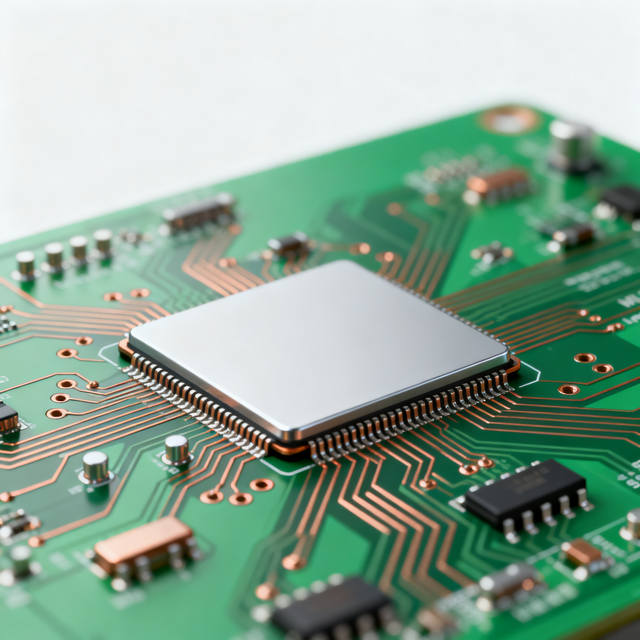
The core concepts of high-speed PCB design revolve around maintaining signal integrity, minimizing electromagnetic interference (EMI), and ensuring efficient power distribution. High-speed designs often involve complex circuit topologies that require precise component placement and routing. The architecture of these PCBs is designed to handle fast data rates, which can lead to issues such as signal distortion and crosstalk if not properly managed. Principles such as controlled impedance, differential signaling, and proper ground plane design are crucial to achieving optimal performance in high-speed circuits.
Detailed Specifications
When designing high-speed PCBs, several specifications are critical to ensure performance and reliability. These include component values, calculations, and formulas that define the electrical characteristics of the circuit. Understanding these parameters helps engineers make informed decisions during the design phase, ultimately leading to more robust and efficient PCBs.
| Parameter | Value/Calculation | Formula/Description |
|---|---|---|
| Resistor Value (R) | 10kΩ | Used for current limiting |
| Capacitor Value (C) | 100nF | Decoupling capacitor for noise reduction |
| Inductor Value (L) | 10μH | Used in filter circuits |
| Voltage (V) | 3.3V | Standard power supply voltage |
| Current (I) | 500mA | Total current consumption |
| Frequency (f) | 2.4GHz | Operating frequency of the circuit |
| Impedance (Z) | 50Ω | Characteristic impedance for matching |
| Signal Rise Time (tr) | 1ns | Time for signal to transition from low to high |
| Trace Width | 0.2mm | Width of PCB trace to maintain impedance |
| Dielectric Constant (εr) | 4.2 | Material property impacting signal speed |
| Thermal Resistance (θja) | 30°C/W | Heat dissipation capability |
Key Takeaways from the Specifications
The specifications outlined in the table are foundational to the design of high-speed PCBs. For instance, the resistor and capacitor values are chosen to optimize current flow and minimize noise, respectively. The impedance value of 50Ω is critical for maintaining signal integrity, especially in RF applications. The thermal resistance indicates the board's ability to dissipate heat, which is essential for preventing component failure. Understanding these parameters allows engineers to tailor their designs to meet specific performance criteria, ensuring reliability and efficiency in their applications.
| Performance Metric | Value | Significance |
|---|---|---|
| Gain | 20dB | Amplification factor of the circuit |
| Bandwidth | 1GHz | Frequency range over which the circuit operates effectively |
| Noise Figure | 3dB | Measure of noise added by the circuit |
| Power Consumption | 1W | Total power used by the circuit |
| Signal-to-Noise Ratio (SNR) | 40dB | Quality of the signal compared to background noise |
| Return Loss | 15dB | Reflection of signals due to impedance mismatches |
| Harmonic Distortion | 0.5% | Measure of signal purity |
| Phase Margin | 45° | Stability of the feedback system |
Practical Implications
The performance metrics are crucial for evaluating the efficacy of a high-speed PCB design. The gain and bandwidth determine the circuit's ability to amplify and process signals over a specific range. A low noise figure and high SNR are indicative of a clean signal, which is vital for applications requiring high precision. Power consumption is a key factor in selecting components for battery-operated devices. Understanding these metrics helps in optimizing the design for specific applications, ensuring that the circuit performs reliably under expected conditions.
| Configuration | Pros | Cons |
|---|---|---|
| Single-Ended | Simple design, low cost | Prone to noise, limited bandwidth |
| Differential | High noise immunity, better performance | Complex design, higher cost |
| Microstrip | Easy to manufacture, good for RF | Higher losses at high frequencies |
| Stripline | Low EMI, balanced structure | Complex manufacturing, costly |
| Grounded Coplanar Waveguide | Low loss, high frequency | Complex design rules, sensitive to changes |
| Embedded Resistors | Space-saving, improved performance | Higher cost, manufacturing complexity |
| Via Stitching | Improved signal integrity, reduced EMI | Increased board complexity, higher cost |
Application Guidelines
Choosing the right configuration for your PCB design involves balancing various trade-offs. Single-ended configurations are cost-effective but may not be suitable for high-speed applications due to noise susceptibility. Differential configurations offer better performance at the expense of complexity and cost. Microstrip and stripline are popular for RF applications, each with its own advantages and limitations. Understanding these trade-offs helps engineers select the most appropriate configuration for their specific requirements, ensuring optimal performance and reliability.
Design Considerations
Designing high-speed PCBs involves several critical considerations. Engineers must account for signal integrity, power distribution, and thermal management. Using differential signaling and controlled impedance helps maintain signal quality. Proper grounding and decoupling techniques are essential for minimizing noise and EMI. Component placement and routing should be optimized to reduce parasitic effects and ensure efficient power delivery. Thermal management strategies, such as using heat sinks and thermal vias, are crucial for preventing overheating and ensuring long-term reliability.
Step-by-Step Implementation
- Define the specifications and requirements of your PCB design, including signal frequency, power levels, and environmental conditions.
- Select appropriate components based on the defined specifications, ensuring they meet the required electrical and thermal performance.
- Design the circuit topology, incorporating techniques such as differential signaling and controlled impedance to enhance signal integrity.
- Layout the PCB, paying attention to trace routing, component placement, and grounding strategies to minimize noise and interference.
- Perform simulations to validate the design, checking for potential issues such as crosstalk, reflection, and power integrity problems.
- Fabricate a prototype of the PCB and conduct thorough testing to evaluate performance against the specified criteria.
- Iterate on the design based on test results, making necessary adjustments to improve performance and reliability.
- Finalize the design for production, ensuring all documentation is complete and compliant with relevant standards, such as IPC-A-610 and IPC-2221.
Common Issues & Solutions
- Signal Integrity Problems: Use controlled impedance and differential signaling to minimize reflections and crosstalk.
- Thermal Management: Implement heat sinks, thermal vias, and proper airflow to manage heat dissipation.
- Electromagnetic Interference: Utilize proper grounding techniques and shielding to reduce EMI.
- Power Integrity Issues: Ensure adequate decoupling and use wide power traces to maintain stable power delivery.
- Component Failure: Select components with appropriate ratings and conduct thorough testing to ensure reliability.
- Manufacturing Defects: Work with reputable manufacturers and follow IPC standards to minimize defects and ensure quality.
Applications & Use Cases
High-speed PCBs are integral to various applications, including telecommunications, computing, and automotive electronics. In telecommunications, they enable fast data transmission in devices such as routers and switches. In computing, they are used in high-performance processors and memory modules. Automotive electronics benefit from high-speed PCBs in advanced driver-assistance systems (ADAS) and infotainment systems, where reliable and fast data processing is essential.
Selection & Sourcing Guide
When selecting components for high-speed PCB designs, it's essential to consider factors such as electrical performance, thermal characteristics, and cost. Utilize resources like IC Online to source components that meet your design requirements. Ensure that the components are from reputable manufacturers and comply with relevant industry standards to guarantee quality and reliability.
FAQ
- What is the importance of controlled impedance in high-speed PCB designs? Controlled impedance is critical for maintaining signal integrity by minimizing reflections and ensuring consistent signal transmission.
- How can I reduce electromagnetic interference in my PCB design? Use proper grounding techniques, shielding, and maintain adequate spacing between traces to reduce EMI.
- Why is differential signaling preferred in high-speed designs? Differential signaling offers better noise immunity and reduces the impact of crosstalk, making it ideal for high-speed applications.
- What role do decoupling capacitors play in PCB design? Decoupling capacitors help stabilize power supply voltages by filtering out noise and providing transient current during switching events.
- How can I ensure thermal management in my PCB design? Implement heat sinks, thermal vias, and ensure proper airflow to manage heat dissipation and prevent overheating.
- What are the common causes of signal integrity issues? Signal integrity issues can arise from factors like impedance mismatches, crosstalk, and inadequate grounding.
- How do I select the right components for my PCB design? Consider factors such as electrical performance, thermal characteristics, and cost when selecting components, and ensure compliance with industry standards.
- What testing methods are essential for high-speed PCB designs? Essential testing methods include signal integrity analysis, power integrity testing, and thermal testing to ensure reliable performance.
- Why is it important to follow IPC standards in PCB design? IPC standards ensure quality, reliability, and manufacturability of PCBs, reducing the likelihood of defects and failures.
- How can I optimize my PCB layout for high-speed applications? Optimize trace routing, use controlled impedance, and maintain proper spacing between components to enhance performance and reliability.
Conclusion
Ensuring the reliability of high-speed PCB designs is a multifaceted challenge that requires careful consideration of specifications, performance metrics, and design trade-offs. By adhering to industry standards and employing rigorous testing methods, engineers can create robust and efficient PCBs that meet the demands of modern electronic applications. Armed with the right knowledge and tools, designers can overcome the complexities of high-speed PCB design, delivering products that perform reliably in the real world.