Essential PCB Layout Design Rules for Optimizing 4-Layer Circuit Boards
Essential PCB Layout Design Rules for Optimizing 4-Layer Circuit Boards Introduction Printed Circuit Boards (PCBs) are the backbone of most electronic devices, providing the physical platform for circ...
Introduction
Printed Circuit Boards (PCBs) are the backbone of most electronic devices, providing the physical platform for circuit components and the interconnections between them. In the realm of modern electronics, 4-layer PCBs offer a balance between complexity and cost, making them ideal for a wide range of applications. With the increasing demand for compact and efficient electronic devices, optimizing the design of 4-layer PCBs is crucial. This article delves into the essential design rules for 4-layer PCB layout, focusing on circuit topology, component calculations, performance analysis, and design trade-offs.
Technical Overview
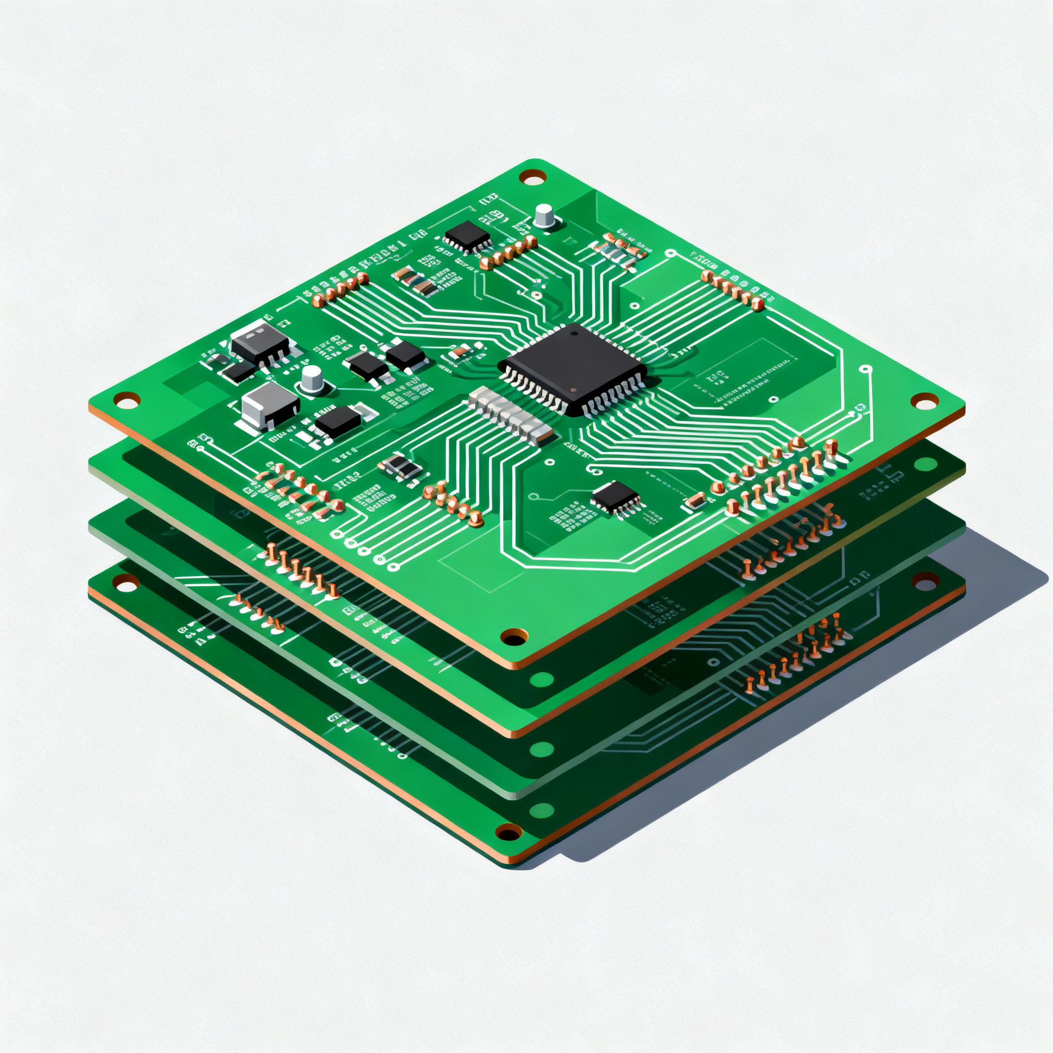
The design of a 4-layer PCB involves several core concepts and principles. The architecture typically consists of two outer layers for component placement and routing, and two inner layers for power and ground planes. This configuration facilitates reduced electromagnetic interference (EMI) and improved signal integrity. Key principles include maintaining controlled impedance, minimizing crosstalk, and ensuring effective thermal management. Understanding these principles is vital for optimizing the performance and reliability of the PCB.
Designing a 4-layer PCB requires a thorough understanding of the electrical and physical characteristics of the components and the board itself. This involves calculating trace widths and spacing, determining the appropriate stack-up, and selecting suitable materials. Additionally, designers must consider the trade-offs between performance, cost, and manufacturability.
Detailed Specifications
Specifications play a critical role in PCB design, dictating the electrical and mechanical parameters that define the board's performance. Essential specifications include component values, trace dimensions, and material properties. These parameters influence the board's ability to handle power, maintain signal integrity, and dissipate heat. Accurate calculations and adherence to industry standards, such as those outlined by the IPC, are crucial for successful PCB design.
| Parameter | Value | Formula/Calculation |
|---|---|---|
| Trace Width | 0.15 mm | Calculated using IPC-2221A |
| Impedance | 50 Ohms | Z = 87/sqrt((Dk+1.41)ln(5.98H/(0.8W+T))) |
| Dielectric Constant (Dk) | 4.2 | Material property |
| Crosstalk | < 3% | Minimize by increasing trace spacing |
| Power Plane Thickness | 1 oz/ft² | Standard thickness for power layers |
| Signal Layer Thickness | 0.5 oz/ft² | Standard thickness for signal layers |
| Thermal Conductivity | 0.8 W/mK | Based on material choice |
| Via Diameter | 0.3 mm | Determined by drill size and plating |
| Stack-up Configuration | Signal-Ground-Power-Signal | Standard 4-layer configuration |
| Clearance | 0.2 mm | IPC-2221A guidelines |
Key Takeaways from the Specifications
The table above outlines critical design parameters that influence the performance and reliability of a 4-layer PCB. Accurate calculation of trace width and impedance ensures signal integrity and minimizes electromagnetic interference. The dielectric constant and thermal conductivity are material properties that affect the board's electrical performance and heat dissipation capabilities. Adhering to IPC standards for via diameter and clearance helps maintain manufacturability and reliability. Understanding these parameters allows designers to make informed decisions during the PCB design process, balancing performance with cost and manufacturability.
| Performance Metric | Value | Impact |
|---|---|---|
| Gain | 15 dB | Determines amplification level |
| Bandwidth | 2 GHz | Defines frequency range |
| Signal-to-Noise Ratio (SNR) | 70 dB | Higher is better for clarity |
| Power Consumption | 5 W | Affects thermal management |
| Return Loss | -20 dB | Indicates signal reflection |
| Insertion Loss | 0.5 dB | Lower loss is preferable |
| Phase Margin | 60° | Stability indicator |
| EMI Emission | < -50 dBm | Lower emissions reduce interference |
| Thermal Resistance | 15 °C/W | Influences heat dissipation |
| Latency | 10 ns | Critical for high-speed applications |
Practical Implications
Performance metrics are crucial in evaluating the effectiveness of a PCB design. Gain and bandwidth determine the board's capability to process signals, while SNR and return loss indicate signal quality. Power consumption and thermal resistance are critical for managing heat and ensuring reliability. Metrics like EMI emission and insertion loss affect the board's electromagnetic compatibility. Understanding these metrics helps engineers optimize the design for specific applications, ensuring that the board meets performance requirements without exceeding cost or power constraints.
| Configuration | Pros | Cons |
|---|---|---|
| Signal-Ground-Power-Signal | Improved signal integrity | Complex routing |
| Power-Ground-Signal-Signal | Efficient power distribution | Higher EMI |
| Signal-Signal-Power-Ground | Cost-effective for simple designs | Poor signal integrity |
| Ground-Signal-Power-Signal | Balanced performance | Moderate complexity |
| Signal-Power-Ground-Signal | Reduced crosstalk | Increased layer cost |
| Power-Signal-Ground-Signal | Good EMI shielding | Complex stack-up |
| Ground-Power-Signal-Signal | Minimal crosstalk | Limited flexibility |
Application Guidelines
Different 4-layer PCB configurations offer unique advantages and disadvantages. The Signal-Ground-Power-Signal configuration provides excellent signal integrity but involves complex routing. Conversely, the Power-Ground-Signal-Signal setup ensures efficient power distribution but may lead to higher EMI. Choosing the right configuration depends on the specific requirements of the application, such as signal integrity, power distribution, and cost constraints. Understanding these trade-offs enables designers to tailor the PCB layout to meet the needs of the final product.
Design Considerations
When designing a 4-layer PCB, several practical guidelines should be followed to ensure optimal performance. Firstly, maintain a clear separation between power and ground planes to minimize noise and improve signal integrity. Use controlled impedance traces for high-speed signals to prevent signal degradation. Ensure adequate spacing between traces to reduce crosstalk and adhere to design rules for minimum trace width and clearance as per IPC standards.
Thermal management is another critical consideration. Use thermal vias and adequate copper thickness to dissipate heat effectively. Components with high power consumption should be placed strategically to minimize thermal hotspots. Signal routing should be optimized to minimize trace lengths and avoid sharp angles, which can cause signal reflections.
Finally, consider the manufacturability of the PCB. Ensure that the design complies with the capabilities of the chosen fabrication process, including minimum drill sizes and layer stack-up options. Collaboration with the PCB manufacturer during the design phase can help identify potential issues and streamline the production process.
Step-by-Step Implementation
- Define the PCB requirements: Identify the electrical and mechanical specifications based on the intended application, including component placement, signal integrity, and thermal management needs.
- Create a schematic: Use CAD software to design the circuit schematic, ensuring all components are correctly represented and connected.
- Select the stack-up: Choose the appropriate 4-layer configuration based on performance requirements, considering trade-offs between signal integrity and cost.
- Design the layout: Place components optimally, taking into account routing complexity and thermal considerations. Route traces with attention to impedance control and signal integrity.
- Conduct design rule checks: Use software tools to verify compliance with design rules, including trace width, spacing, and clearance. Ensure adherence to IPC standards.
- Simulate the design: Perform simulations to validate signal integrity, power distribution, and thermal performance. Make adjustments as necessary based on simulation results.
- Prepare fabrication files: Generate Gerber files and other necessary documentation, ensuring all design details are accurately captured for manufacturing.
- Collaborate with the manufacturer: Work closely with the PCB manufacturer to address any potential issues and optimize the design for production.
Common Issues & Solutions
- Signal Integrity Problems: Use controlled impedance routing and increase trace spacing to reduce crosstalk and reflections.
- Thermal Management Challenges: Incorporate thermal vias and optimize copper thickness to enhance heat dissipation.
- EMI Concerns: Implement proper grounding techniques and shield sensitive traces to minimize electromagnetic interference.
- Manufacturability Issues: Ensure design rules align with manufacturing capabilities, and engage with the manufacturer early in the design process.
- Component Placement Conflicts: Use CAD tools to visualize and optimize component placement for efficient routing and thermal performance.
- Power Distribution Inefficiencies: Design power planes with adequate thickness and minimize via inductance to ensure stable power delivery.
Applications & Use Cases
4-layer PCBs are widely used in various applications due to their balance of performance and cost. They are commonly found in consumer electronics, such as smartphones and tablets, where compact size and high performance are essential. Industrial control systems and automotive electronics also benefit from the enhanced signal integrity and power distribution capabilities of 4-layer PCBs. In telecommunications, these boards are used in networking equipment to manage high-speed data transmission. The versatility of 4-layer PCBs makes them suitable for a broad range of applications, from simple devices to complex systems.
Selection & Sourcing Guide
When selecting components and sourcing PCBs, it is essential to consider the quality and reliability of the suppliers. Visit IC Online for a comprehensive selection of integrated circuits and electronic components from reputable manufacturers. Collaborating with trusted suppliers ensures that the components meet the required specifications and standards, enhancing the overall performance and reliability of the PCB.
FAQ
- What are the advantages of a 4-layer PCB over a 2-layer PCB? A 4-layer PCB offers improved signal integrity, reduced EMI, and better power distribution compared to a 2-layer PCB, making it suitable for more complex and high-performance applications.
- How do I calculate the impedance of a trace? Impedance can be calculated using formulas that consider trace width, thickness, dielectric constant, and separation from the ground plane. Tools and calculators based on IPC-2221A standards are available for precise calculations.
- What is the role of the dielectric constant in PCB design? The dielectric constant affects the impedance and signal speed of traces. Selecting materials with appropriate dielectric properties is crucial for maintaining signal integrity.
- How can I minimize crosstalk on a 4-layer PCB? Increase trace spacing, use ground planes to isolate signal layers, and route high-speed signals on inner layers to reduce crosstalk.
- What factors influence power consumption on a PCB? Power consumption is influenced by component selection, trace resistance, and thermal management. Efficient power plane design and component placement can help optimize power usage.
- Why is thermal management important in PCB design? Effective thermal management prevents overheating, which can lead to component failure and reduced reliability. It ensures that the device operates within safe temperature limits.
- How do I choose the right stack-up for my 4-layer PCB? The stack-up should be chosen based on performance requirements, considering factors like signal integrity, power distribution, and EMI. Evaluate trade-offs between different configurations to meet application needs.
- What are the common materials used for 4-layer PCBs? Common materials include FR-4, which is widely used for its balance of performance and cost. High-frequency applications may require specialized materials with lower dielectric losses.
- How can I ensure my PCB design is manufacturable? Follow design rules that align with the capabilities of your chosen PCB manufacturer, and engage in early collaboration to address potential fabrication challenges.
- What tools are available for PCB design and simulation? Popular PCB design tools include Altium Designer, Eagle, and KiCad. Simulation tools like SPICE and HyperLynx can be used to validate electrical performance.
Conclusion
Optimizing the design of a 4-layer PCB involves a careful balance of performance, cost, and manufacturability. By adhering to essential design rules and understanding the trade-offs involved, engineers can create PCBs that meet the specific needs of their applications. The insights provided in this article serve as a comprehensive guide for designing effective and reliable 4-layer PCBs, ensuring that they deliver optimal performance in real-world conditions.