Essential PCB Design Guidelines: Key Considerations for Optimal Performance
Essential PCB Design Guidelines: Key Considerations for Optimal Performance Introduction In the rapidly evolving world of electronics, the printed circuit board (PCB) remains a cornerstone of design a...
Introduction
In the rapidly evolving world of electronics, the printed circuit board (PCB) remains a cornerstone of design and functionality. With the increasing demand for high-performance, compact, and reliable electronics, understanding essential PCB design guidelines is critical for engineers and designers. This article delves into the core aspects of PCB design, focusing on RF components—highlighting component specifications, selection criteria, and application circuits. By adhering to industry standards and utilizing the right design strategies, you can ensure optimal performance and reliability of your electronic products.
Technical Overview
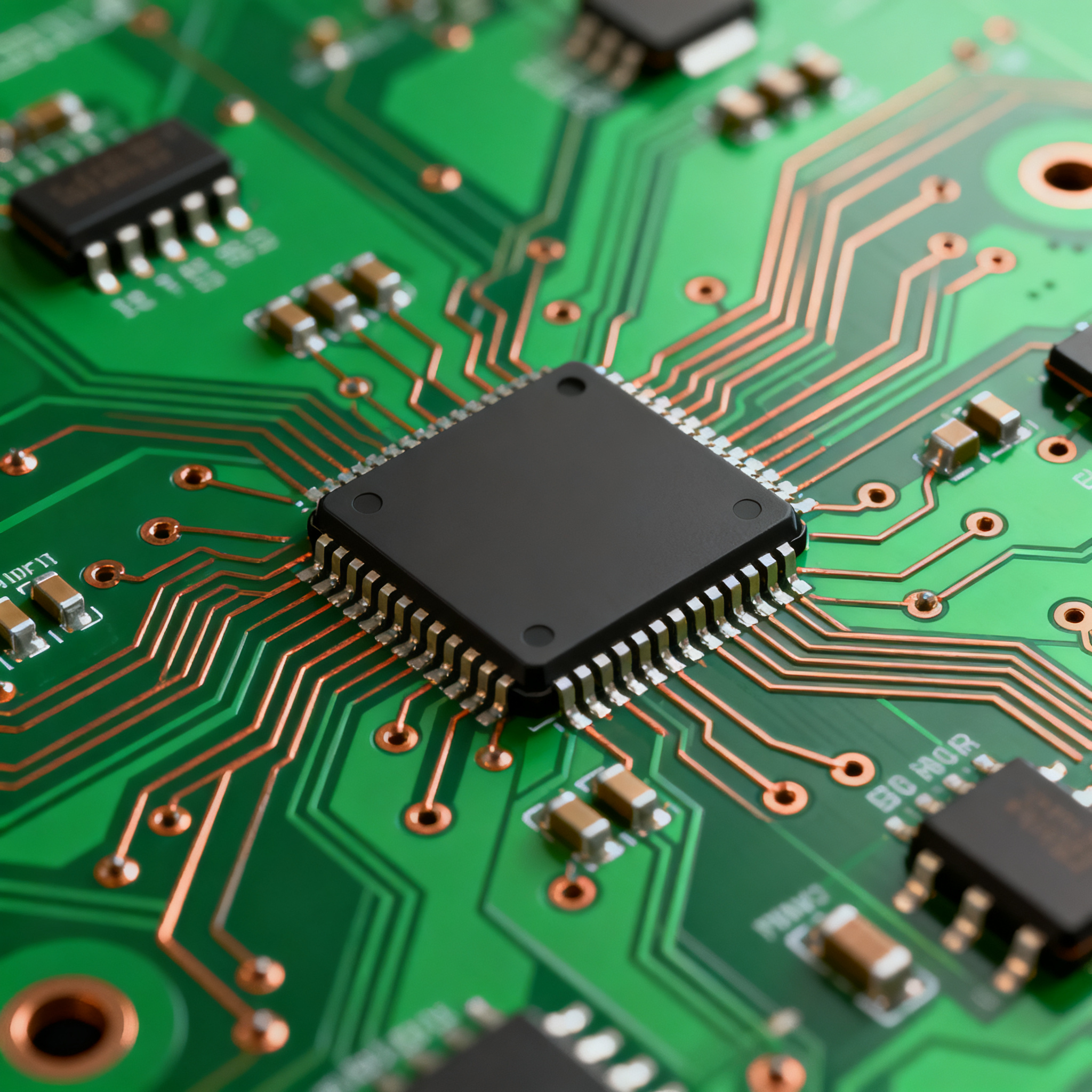
PCBs serve as the backbone of electronic devices, providing mechanical support and electrical connections for components. At their core, PCBs are composed of multiple layers, each serving a specific function—whether it's carrying a signal, providing a ground plane, or serving as a power plane. The design of a PCB is governed by several principles, including trace routing, component placement, and thermal management. For RF components, additional considerations such as impedance matching, signal integrity, and electromagnetic compatibility (EMC) must be taken into account.
The architecture of a PCB can vary greatly depending on the application, ranging from single-layer boards for basic applications to multi-layer boards for complex systems. Design principles such as controlled impedance, proper grounding, and minimizing parasitic inductance and capacitance are crucial for maintaining signal integrity, especially in high-frequency applications. By understanding these core concepts, engineers can craft PCBs that not only meet functional requirements but also excel in performance and reliability.
Detailed Specifications
When designing PCBs, especially for RF applications, paying close attention to component specifications is paramount. Key specifications include parameters such as operating frequency, power handling, and size constraints. Understanding these specifications helps in selecting the right components that align with your design goals and constraints. Below is a table detailing some of the key specifications to consider when selecting RF components for PCB design.
| Parameter | Description | Typical Values |
|---|---|---|
| Operating Frequency | The frequency range over which the component operates effectively. | DC to 3 GHz |
| Power Handling | The maximum power level the component can handle. | 1W to 10W |
| Insertion Loss | The loss of signal power resulting from the insertion of a device in a transmission line. | 0.1 dB to 0.5 dB |
| Return Loss | The loss of power in the signal returned/reflected by a discontinuity in a transmission line. | 15 dB to 30 dB |
| Isolation | The ability to prevent RF leakage between ports. | 20 dB to 50 dB |
| Size | Physical dimensions of the component. | 1mm x 1mm to 10mm x 10mm |
| Temperature Range | The range of temperatures over which the component can operate reliably. | -40°C to 85°C |
| Impedance | The resistance to the flow of alternating current, measured in ohms. | 50 Ohms |
| Voltage Rating | The maximum voltage the component can withstand. | 5V to 30V |
| Capacitance | The ability of the component to store an electric charge. | 0.1pF to 10pF |
Key Takeaways from the Specifications
Understanding the specifications outlined in the table above is critical for selecting the right RF components for your PCB design. The operating frequency and power handling capabilities dictate the component's suitability for specific applications. Insertion and return losses are crucial for signal integrity, especially in high-frequency designs. Size constraints and temperature ranges are practical considerations that impact the physical layout and environmental resilience of the PCB. By carefully analyzing these parameters, engineers can ensure that the chosen components align with the overall design objectives and operational requirements.
| Metric | Description | Typical Values |
|---|---|---|
| Signal-to-Noise Ratio (SNR) | The ratio of signal power to noise power, indicating signal clarity. | 30 dB to 50 dB |
| Gain | The increase in power or amplitude of a signal. | 10 dB to 20 dB |
| Bandwidth | The range of frequencies over which the component can operate effectively. | 100 MHz to 1 GHz |
| Efficiency | The ratio of output power to input power, expressed as a percentage. | 60% to 90% |
| Harmonic Distortion | The presence of harmonics in the output signal. | -30 dBc to -60 dBc |
| Phase Noise | The frequency stability of the signal. | -100 dBc/Hz at 1 kHz offset |
| Thermal Resistance | The resistance to heat flow within the component. | 10°C/W to 30°C/W |
| Rise Time | The time it takes for a signal to change from low to high. | 1 ns to 10 ns |
| Current Consumption | The amount of current the component draws during operation. | 10 mA to 100 mA |
Practical Implications
The performance metrics listed above are crucial for evaluating the effectiveness of RF components within a PCB design. Metrics such as signal-to-noise ratio (SNR) and gain are indicative of the component's ability to amplify and maintain signal integrity. Bandwidth and efficiency are key for ensuring the component can handle the necessary frequency range and power consumption requirements. Thermal resistance and current consumption are critical for thermal management and energy efficiency, particularly in high-power applications. By understanding these metrics, engineers can make informed decisions that optimize the performance and reliability of their PCBs.
| Application | Configuration | Key Considerations |
|---|---|---|
| Wireless Communication | Transceiver Module | Impedance Matching, Low Insertion Loss |
| Radar Systems | Antenna Array | High Isolation, Phase Noise |
| Consumer Electronics | RF Amplifier | Efficiency, Thermal Management |
| Automotive | Telematics Unit | Temperature Range, Vibration Resistance |
| Medical Devices | Wireless Sensor | Size Constraints, Power Handling |
| Industrial Automation | RFID Reader | Bandwidth, Current Consumption |
| Aerospace | Satellite Communication | Radiation Hardening, Reliability |
Application Guidelines
The application matrix provided above illustrates the diverse range of use cases for RF components in PCB design. Each application has specific configuration requirements and key considerations. For instance, wireless communication systems prioritize impedance matching and low insertion loss to maintain signal integrity. Radar systems, on the other hand, require high isolation and low phase noise to ensure accurate signal processing. By understanding these application-specific needs, engineers can tailor their PCB designs to meet the unique demands of each use case, ultimately leading to more efficient and reliable electronic systems.
Design Considerations
When embarking on PCB design, especially for RF applications, several critical considerations must be addressed to ensure optimal performance. First and foremost, trace routing is a key aspect that influences signal integrity. Properly routed traces minimize parasitic inductance and capacitance, which are detrimental to high-frequency signals. Additionally, maintaining consistent controlled impedance throughout the board is crucial for preventing signal reflections and ensuring signal integrity.
Component placement is another vital consideration. Placing components too close to each other can lead to unwanted coupling and interference. It's essential to maintain adequate spacing between components, especially in RF designs, to minimize electromagnetic interference (EMI). Grounding strategies also play a significant role in PCB design. A well-designed ground plane reduces EMI and crosstalk, thereby enhancing the overall performance of the PCB.
Thermal management is also critical, especially for high-power applications. Adequate heat dissipation through the use of thermal vias, heat sinks, and copper pours ensures that components operate within their specified temperature ranges. By addressing these design considerations, engineers can create PCBs that not only meet functional requirements but also excel in performance and reliability.
Step-by-Step Implementation
- Define Requirements: Begin by clearly defining the requirements of your PCB, including the operating frequency, power handling, and size constraints. This will guide your component selection and design decisions.
- Select Components: Based on the defined requirements, select RF components that meet the necessary specifications. Pay close attention to parameters such as impedance, insertion loss, and thermal performance.
- Design Schematic: Create a detailed schematic of the PCB, ensuring that all components are correctly connected and that signal paths are optimized for performance.
- Place Components: Strategically place components on the PCB layout, maintaining adequate spacing to minimize interference and facilitate efficient trace routing.
- Route Traces: Route traces with controlled impedance, minimizing length and avoiding sharp angles to reduce signal reflections and losses.
- Implement Grounding: Design a robust grounding strategy, utilizing ground planes and vias to reduce EMI and enhance signal integrity.
- Conduct Thermal Analysis: Perform a thermal analysis to ensure that heat dissipation strategies are adequate for the power levels and operating conditions of the PCB.
- Prototype and Test: Fabricate a prototype of the PCB and conduct thorough testing to validate performance metrics and identify any areas for improvement.
Common Issues & Solutions
In PCB design, several common issues can arise, particularly in RF applications. Here are some real problems and their solutions:
- Signal Integrity Issues: Poor signal integrity can result from improper trace routing. Solution: Ensure controlled impedance and minimize trace lengths.
- Electromagnetic Interference (EMI): EMI can degrade performance. Solution: Implement proper grounding and shielding strategies.
- Thermal Management Challenges: Overheating can damage components. Solution: Use thermal vias and heat sinks to enhance heat dissipation.
- Component Sourcing Delays: Delays in sourcing components can affect timelines. Solution: Utilize multiple suppliers and maintain a buffer stock.
- Design Rule Violations: Violations can occur due to oversight. Solution: Use design rule checks (DRC) in PCB design software to catch errors early.
Applications & Use Cases
RF components in PCB designs have a wide range of applications across various industries. In wireless communication, they are used in transceivers for mobile phones and Wi-Fi routers. Radar systems in automotive and aerospace applications rely heavily on RF components for detecting objects and measuring speed. In consumer electronics, RF amplifiers enhance signal strength in devices like televisions and radios. The medical field utilizes RF components in wireless sensors for patient monitoring, while industrial automation systems use them in RFID readers for inventory tracking. Each application presents unique challenges and requirements, making it essential to tailor PCB designs accordingly.
Selection & Sourcing Guide
Selecting and sourcing RF components for PCB design requires careful consideration of specifications and availability. Utilize resources like IC Online to find components that meet your design criteria. Compare datasheets to ensure compatibility with your design requirements, and consider factors such as lead times and supplier reliability. Establishing relationships with multiple suppliers can mitigate risks associated with component shortages and ensure a steady supply chain.
FAQ
- Q: What is controlled impedance?
A: Controlled impedance refers to maintaining a consistent resistance to alternating current in PCB traces, essential for signal integrity in high-frequency designs. - Q: Why is grounding important in PCB design?
A: Grounding reduces electromagnetic interference (EMI) and enhances signal integrity by providing a reference point for signals. - Q: How can I minimize EMI in my PCB design?
A: Use ground planes, maintain adequate spacing between components, and implement shielding to minimize EMI. - Q: What are thermal vias?
A: Thermal vias are small holes in the PCB that allow heat to flow from the surface to inner layers, enhancing heat dissipation. - Q: How do I choose the right RF component for my application?
A: Consider factors such as operating frequency, power handling, and size constraints to select components that meet your design needs. - Q: What is insertion loss?
A: Insertion loss is the loss of signal power resulting from the insertion of a device in a transmission line, measured in decibels (dB). - Q: How can I ensure signal integrity in my PCB design?
A: Maintain controlled impedance, minimize trace lengths, and avoid sharp angles in trace routing. - Q: What is the significance of return loss?
A: Return loss indicates the amount of signal power reflected due to impedance mismatches, impacting signal integrity. - Q: Why is component placement critical in RF PCB design?
A: Proper placement minimizes unwanted coupling and interference, ensuring optimal performance. - Q: What resources are available for PCB design standards?
A: IPC Standards provide comprehensive guidelines for PCB design, assembly, and quality inspection.
Conclusion
In conclusion, adhering to essential PCB design guidelines is crucial for achieving optimal performance, particularly in RF applications. By understanding and applying the right specifications, performance metrics, and application considerations, engineers can design PCBs that meet the demands of modern electronic systems. With a focus on signal integrity, thermal management, and component selection, this article provides a comprehensive guide to navigating the complexities of PCB design, ensuring that your products perform reliably and efficiently in real-world applications.