Essential Equipment for Efficient 4-Layer PCB Assembly: A Practical Guide
Essential Equipment for Efficient 4-Layer PCB Assembly: A Practical Guide Introduction In today's rapidly evolving electronics industry, 4-layer PCBs have become a staple in ensuring efficient and com...
Introduction
In today's rapidly evolving electronics industry, 4-layer PCBs have become a staple in ensuring efficient and compact design for complex circuits. With the growth of IoT, automotive electronics, and consumer devices, the need for precise and efficient PCB assembly cannot be overstated. This guide focuses on essential equipment and methodologies for assembling 4-layer PCBs, emphasizing component specifications, datasheets, selection criteria, and application circuits. Understanding these elements is crucial for engineers and manufacturers to produce high-quality, reliable products that meet industry standards such as those set by IPC.
Technical Overview
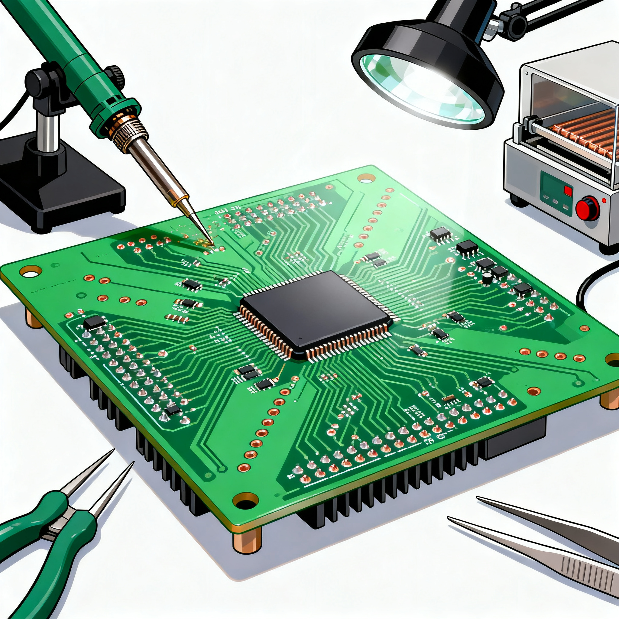
4-layer PCBs are a fundamental part of modern electronics. They offer enhanced electrical performance and reduced electromagnetic interference, making them ideal for high-speed and high-frequency applications. The architecture of a 4-layer PCB typically includes a signal layer, ground plane, power plane, and another signal layer. This configuration provides a robust platform for complex circuits and allows for efficient routing of signals. The principles of designing a 4-layer PCB involve careful consideration of impedance control, thermal management, and signal integrity. By adhering to IPC standards and leveraging resources from manufacturers like PCBWay and Nova PCBA, engineers can ensure their designs meet both performance and reliability criteria.
Detailed Specifications
When selecting components for a 4-layer PCB, several specifications are crucial. These include CPU speed, memory capacity, peripheral interfaces, power requirements, and package type. Understanding these specifications helps in choosing the right components that fit the design's performance and physical constraints.
| Specification | Detail | Importance |
|---|---|---|
| CPU Speed | 1.2 GHz | High processing speed for complex tasks |
| Memory | 256 MB RAM | Ample memory for data handling |
| Peripherals | USB, I2C, SPI | Multiple interfacing options |
| Power Supply | 3.3V, 5V | Common voltage levels for compatibility |
| Package Type | LQFP, BGA | Variety of packaging for different applications |
| Operating Temperature | -40°C to 85°C | Wide range for various environments |
| Dimensions | 10mm x 10mm | Compact size for integration |
| Weight | 2g | Lightweight for portable devices |
Key Takeaways from the Specifications
The core specifications of a component are critical in determining its suitability for a specific application. CPU speed and memory size are pivotal for performance-intensive tasks, while the availability of peripheral interfaces like USB, I2C, and SPI ensures connectivity and flexibility. Power supply requirements must align with the overall system design to ensure efficiency and reliability. The package type affects the ease of assembly and the footprint on the PCB, with options like LQFP and BGA offering different benefits. Understanding these specifications is essential for selecting components that meet both functional and physical constraints of your design.
| Electrical Parameter | Value | Significance |
|---|---|---|
| Operating Voltage | 3.3V | Standard for many digital circuits |
| Current Consumption | 50 mA | Low power usage for efficiency |
| Input Logic Level | 0.8V (Low), 2.0V (High) | Defines digital signal thresholds |
| Output Logic Level | 0.4V (Low), 2.4V (High) | Ensures compatibility with other ICs |
| Clock Frequency | 100 MHz | Determines timing and processing speed |
| Propagation Delay | 5 ns | Impacts signal timing and synchronization |
| Thermal Resistance | 20°C/W | Important for thermal management |
| ESD Protection | ±2 kV | Prevents damage from electrostatic discharge |
Practical Implications
Electrical characteristics dictate the interaction of components within the PCB environment. Operating voltage and current consumption are crucial for power management, affecting both battery life and thermal performance. Input and output logic levels ensure signal compatibility across different ICs, critical for seamless communication. Clock frequency and propagation delay influence the speed and timing of operations, which are vital for high-speed applications. Thermal resistance and ESD protection are key for maintaining component integrity under varying conditions, providing resilience against thermal and electrostatic stresses.
| Application | Configuration | Benefits |
|---|---|---|
| Consumer Electronics | Standard configuration with basic peripherals | Cost-effective and efficient |
| Automotive Systems | Enhanced thermal management and ESD protection | Durability in harsh environments |
| Industrial Control | High CPU speed and memory | Handles complex processing tasks |
| IoT Devices | Low power consumption and compact size | Extended battery life and portability |
| Medical Devices | High reliability and precision | Ensures patient safety and accuracy |
Application Guidelines
Understanding the application context is essential for selecting the right configuration of a 4-layer PCB. Consumer electronics benefit from standard configurations that balance cost and performance, while automotive systems require enhanced features to withstand harsh conditions. Industrial control systems demand high processing power and memory, suitable for complex operations. IoT devices prioritize low power consumption and compactness, essential for portable and battery-operated gadgets. In medical devices, reliability and precision are paramount, ensuring safety and accuracy in critical applications.
Design Considerations
Designing a 4-layer PCB requires careful attention to several key factors to ensure optimal performance and reliability. First, signal integrity must be maintained by proper layer stacking and impedance control. Ground and power planes should be placed adjacent to signal layers to minimize noise and improve EMI performance. Thermal management is also critical; adequate thermal vias and copper pours can help dissipate heat effectively.
Component placement plays a significant role in the overall performance of the PCB. Critical components should be placed close to each other to minimize trace lengths and reduce parasitic inductance and capacitance. Power delivery networks need to be robust, providing stable voltage levels across the board, which can be achieved through proper decoupling and bypass capacitors.
Adherence to design rules and standards, such as those outlined by IPC, is essential. These rules guide everything from trace width and spacing to via design and solder mask clearance. Utilizing tools and resources from manufacturers like PCBWay and Nova PCBA can aid in ensuring these standards are met, providing a foundation for high-quality PCB production.
Step-by-Step Implementation
- Define Requirements: Begin by outlining the functional and performance requirements of your PCB. This includes the intended application, environmental conditions, and any specific regulatory standards that must be met.
- Schematic Design: Develop a detailed schematic diagram that captures all the components and their interconnections. Use schematic capture software to ensure accuracy and consistency.
- Component Selection: Choose components based on the specifications outlined earlier, ensuring they meet the design's electrical and physical requirements. Refer to datasheets for detailed information.
- PCB Layout: Use PCB design software to create the layout, paying attention to component placement, trace routing, and layer stacking. Ensure that signal integrity and thermal management considerations are incorporated.
- Design Review: Conduct a thorough design review to catch any errors or potential issues. This includes checking for electrical rule violations, ensuring adequate clearances, and verifying signal integrity.
- Prototype Fabrication: Send the design to a PCB fabrication service like PCBWay for prototype production. This allows for testing and validation before full-scale manufacturing.
- Testing and Validation: Perform comprehensive testing on the prototype to ensure it meets all functional and performance criteria. This includes electrical testing, thermal analysis, and EMI/EMC testing.
- Production and Assembly: Once the design is validated, proceed with full-scale production and assembly, ensuring that quality control measures are in place to maintain consistency and reliability.
Common Issues & Solutions
- Signal Integrity Problems: These can arise from improper trace routing or layer stacking. Solution: Use controlled impedance lines and keep signal paths short and direct.
- Thermal Management Challenges: Overheating can affect performance and reliability. Solution: Implement adequate thermal vias and copper pours for heat dissipation.
- EMI/EMC Compliance: Failing to meet EMI/EMC standards can result in interference issues. Solution: Use proper shielding techniques and ground planes to reduce emissions.
- Component Placement Errors: Incorrect placement can lead to inefficient routing and signal degradation. Solution: Place critical components close together and minimize trace lengths.
- Power Distribution Issues: Voltage drops and power fluctuations can occur. Solution: Ensure a robust power delivery network with appropriate decoupling capacitors.
Applications & Use Cases
4-layer PCBs are versatile and find applications across various industries. In consumer electronics, they enable compact designs for smartphones and tablets. Automotive systems benefit from their enhanced durability and thermal management, making them suitable for engine control units and infotainment systems. Industrial control applications leverage their processing power for automation and robotics. IoT devices utilize 4-layer PCBs for their low power consumption and small form factor, essential for wearable technology and smart home devices. In the medical field, their reliability and precision support critical applications like diagnostic equipment and patient monitoring systems.
Selection & Sourcing Guide
When selecting and sourcing components for a 4-layer PCB, consider factors such as availability, lead time, and cost. Utilize reputable distributors and manufacturers to ensure component quality and authenticity. For a comprehensive selection of integrated circuits, visit IC Online for a wide range of options.
FAQ
- What is the primary benefit of a 4-layer PCB over a 2-layer PCB?
4-layer PCBs offer improved electrical performance and reduced electromagnetic interference, making them suitable for high-speed and high-frequency applications. - How do I ensure signal integrity in a 4-layer PCB design?
Maintain proper layer stacking, use controlled impedance lines, and keep signal traces short and direct. - What are the common applications of 4-layer PCBs?
They are used in consumer electronics, automotive systems, industrial control, IoT devices, and medical equipment. - What considerations should I make for thermal management?
Implement thermal vias, copper pours, and adequate spacing to facilitate heat dissipation. - How can I minimize EMI/EMC issues in my design?
Use proper shielding techniques, ground planes, and ensure compliance with relevant standards. - What are the typical specifications to look for in a component datasheet?
CPU speed, memory, peripherals, power requirements, and electrical characteristics such as voltage and current. - How can I source reliable components for my PCB?
Use reputable distributors and manufacturers, and consider platforms like IC Online. - What is the importance of adhering to IPC standards?
IPC standards ensure consistency, quality, and reliability in PCB design and manufacturing. - Can 4-layer PCBs be used in wearable devices?
Yes, their compact size and low power consumption make them ideal for wearable technology. - What tools can assist in 4-layer PCB design?
Use PCB design software for schematic capture and layout, and leverage resources from manufacturers like PCBWay and Nova PCBA.
Conclusion
4-layer PCBs are integral to modern electronics, offering enhanced performance and reliability. By understanding component specifications, electrical characteristics, and application requirements, engineers can design and assemble efficient PCBs that meet industry standards. Leveraging resources from manufacturers and adhering to best practices ensures high-quality results that meet the demands of various applications, from consumer electronics to industrial systems.