Introduction
In the realm of high-stakes electronics projects, ensuring the quality of Printed Circuit Board Assemblies (PCBAs) is non-negotiable. These assemblies are the backbone of electronic devices, influencing performance, reliability, and longevity. In industries such as aerospace, medical devices, and telecommunications, the stakes are even higher, where failure can have catastrophic consequences. This article delves into effective quality control measures tailored for PCBAs, focusing on essential design rules, stackup configurations, signal integrity, and manufacturing considerations. By adhering to stringent standards, engineers can mitigate risks, enhance performance, and ensure the success of high-stakes projects.
Technical Overview
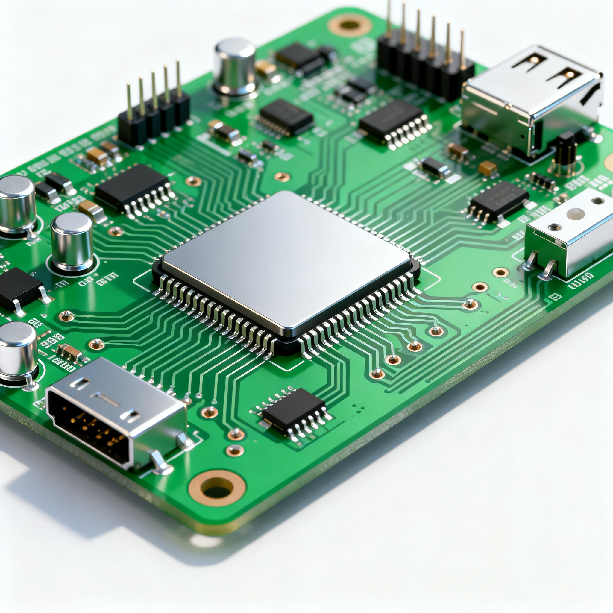
Printed Circuit Board Assemblies (PCBAs) are complex structures that require meticulous design and manufacturing processes. At the core are the PCB layout rules, which dictate the arrangement of components and traces on the board. These rules are essential for ensuring electrical performance and manufacturability.
Signal integrity is another critical aspect, influenced by factors like trace impedance, crosstalk, and electromagnetic interference. Proper stackup design is fundamental to maintaining signal integrity, as it determines the arrangement of layers and the materials used. High-speed designs, in particular, demand precise control over these parameters to prevent signal degradation.
Manufacturing considerations encompass the entire lifecycle of the PCBA, from material selection to assembly processes. Adhering to industry standards such as IPC-A-610 and IPC-2221 ensures that the boards meet stringent quality and reliability criteria. These standards guide everything from trace width and spacing to via sizes and clearances, ensuring that the finished product can withstand the demands of its intended application.
Detailed Specifications
In high-stakes projects, detailed specifications are the foundation of a successful PCBA. These specifications include design rules, stackup options, and material properties, each playing a crucial role in the board's performance and reliability. Understanding these elements is essential for engineers aiming to optimize their designs for specific applications.
| Design Parameter | Minimum Value | Typical Value |
| Trace Width | 5 mil | 8 mil |
| Trace Spacing | 4 mil | 6 mil |
| Via Diameter | 0.2 mm | 0.4 mm |
| Annular Ring | 0.1 mm | 0.15 mm |
| Clearance to Edge | 0.5 mm | 0.8 mm |
| Pad Size for SMT | 0.3 mm | 0.5 mm |
| Drill Hole Size | 0.2 mm | 0.3 mm |
| Solder Mask Clearance | 0.05 mm | 0.1 mm |
| Silkscreen Line Width | 0.1 mm | 0.2 mm |
| Aspect Ratio | 6:1 | 8:1 |
| Impedance Control | ±5% | ±10% |
Key Takeaways from the Specifications
The data presented in the table above outlines critical design parameters that influence PCBA performance. For instance, trace width and spacing are vital for ensuring adequate current-carrying capacity and minimizing crosstalk. A narrower trace width can lead to increased resistance and potential overheating, while insufficient spacing may result in short circuits or signal interference. Via sizes and annular rings are crucial for ensuring reliable electrical connections between layers, especially in multi-layer boards. These specifications are not merely guidelines but are essential for achieving a balance between performance, manufacturability, and cost.
| Stackup Configuration | Number of Layers | Typical Application |
| Single Layer | 1 | Simple circuits |
| Double Layer | 2 | Consumer electronics |
| Four Layer | 4 | Moderate complexity devices |
| Six Layer | 6 | High-speed circuits |
| Eight Layer | 8 | Advanced computing |
| Ten Layer | 10 | Telecommunications |
| Twelve Layer | 12 | Aerospace applications |
| Fourteen Layer | 14 | Critical systems |
Practical Implications
The choice of layer stackup configuration significantly impacts the board's functionality and cost. A single-layer stackup is cost-effective and suitable for simple applications, whereas multi-layer configurations are essential for complex and high-speed designs. As the number of layers increases, so do the manufacturing complexity and cost. However, this allows for more intricate routing and improved signal integrity, crucial for high-frequency applications. Engineers must balance the need for additional layers against the project's budget and performance requirements, ensuring that the chosen stackup meets the specific demands of the application.
| Material | Dielectric Constant (Dk) | Loss Tangent |
| FR-4 | 4.5 | 0.020 |
| Rogers 4350B | 3.66 | 0.0037 |
| Rogers 5880 | 2.20 | 0.0009 |
| Polyimide | 3.5 | 0.004 |
| PTFE (Teflon) | 2.1 | 0.001 |
| Isola 370HR | 4.04 | 0.019 |
| Nelco N4000-13 | 3.9 | 0.009 |
| Arlon 85N | 3.5 | 0.0045 |
| Panasonic Megtron 6 | 3.4 | 0.002 |
| Flexible Kapton | 3.2 | 0.0025 |
Application Guidelines
Material selection is a critical factor in PCBA design, influencing both electrical performance and environmental suitability. FR-4 is a popular choice for general applications due to its balanced dielectric properties and cost-effectiveness. For high-frequency applications, materials like Rogers 4350B and PTFE (Teflon) offer lower dielectric constants and loss tangents, reducing signal attenuation. Polyimide and flexible Kapton are preferred for flexible circuits, offering excellent thermal stability. Engineers must carefully evaluate the dielectric constant and loss tangent of materials to ensure optimal performance for the intended application, considering factors such as signal speed, thermal requirements, and mechanical flexibility.
Design Considerations
Designing a high-quality PCBA involves several critical considerations that ensure optimal performance and reliability. First and foremost, adherence to industry standards such as IPC-A-610 and IPC-2221 is crucial for maintaining consistency and quality. These standards provide guidelines on everything from trace widths and spacing to solder mask and silkscreen requirements.
Signal integrity is another key consideration, particularly in high-speed designs. Engineers must carefully manage trace impedance, crosstalk, and electromagnetic interference to prevent signal degradation. This often involves selecting the appropriate layer stackup and materials, as well as implementing design techniques such as controlled impedance and differential pair routing.
Thermal management is also an essential aspect of design, especially in applications with high power density. Proper heat dissipation can be achieved through the use of thermal vias, heat sinks, and appropriate component placement.
Manufacturability should not be overlooked, as complex designs can lead to increased production costs and longer lead times. It's important to collaborate closely with manufacturing partners to ensure that the design is optimized for efficient production.
Finally, thorough testing and validation are vital to confirm that the design meets all performance and reliability requirements. This includes both electrical testing and environmental testing to assess the board's behavior under various conditions.
Step-by-Step Implementation
Implementing a successful PCBA design involves a series of methodical steps:
- Define Requirements: Clearly outline the performance, reliability, and cost targets for the PCBA based on the project's needs.
- Choose Materials: Select appropriate materials considering dielectric properties, thermal performance, and environmental conditions.
- Design Layout: Create the PCB layout, adhering to design rules and ensuring optimal trace routing for signal integrity.
- Stackup Configuration: Determine the layer stackup that best suits the application, balancing complexity and cost.
- Simulation and Analysis: Use simulation tools to assess signal integrity, thermal performance, and mechanical stability.
- Prototype Development: Collaborate with manufacturing partners to produce a prototype for initial testing and validation.
- Testing and Validation: Conduct thorough testing to verify electrical performance and environmental resilience.
- Iterate and Optimize: Refine the design based on test results, addressing any identified issues before final production.
Common Issues & Solutions
Even with meticulous planning, issues can arise during the PCBA design and manufacturing process. Here are some common problems and their solutions:
- Trace Overheating: Increase trace width or use thicker copper layers to improve current-carrying capacity.
- Signal Crosstalk: Implement proper spacing between traces and use ground planes to reduce interference.
- Impedance Mismatch: Utilize controlled impedance techniques and ensure consistent trace geometries.
- Thermal Management: Employ thermal vias, heat sinks, and strategic component placement for efficient heat dissipation.
- Manufacturing Defects: Work closely with manufacturers to ensure design is optimized for production, and conduct thorough inspections.
- Environmental Stress: Select materials with suitable thermal and mechanical properties to withstand environmental conditions.
Applications & Use Cases
PCBAs are utilized across a wide range of industries, each with unique requirements. In aerospace, they are used in avionics systems where reliability and performance are paramount. Medical devices rely on PCBAs for precise and reliable operation, often in life-critical applications. In telecommunications, PCBAs enable high-speed data processing and transmission, requiring exceptional signal integrity. Consumer electronics benefit from cost-effective yet high-performance PCBAs, driving innovation in everyday devices. Each use case demands careful consideration of design, materials, and manufacturing processes to meet specific industry standards and application needs.
Selection & Sourcing Guide
For sourcing components and materials, it's crucial to partner with reputable suppliers who can provide quality assurance and support.
IC Online is a valuable resource for sourcing electronic components, offering a wide selection and reliable delivery. When selecting suppliers, consider factors such as lead times, certifications, and customer support to ensure a smooth supply chain.
FAQ
- What are the key factors in PCBA design? Key factors include adherence to design rules, signal integrity, thermal management, and manufacturability.
- How do I choose the right stackup configuration? Consider the application's complexity, signal integrity requirements, and budget constraints.
- What materials are best for high-frequency applications? Materials like Rogers 4350B and PTFE offer low dielectric constants and loss tangents, ideal for high-frequency designs.
- How can I ensure signal integrity? Implement controlled impedance, differential pair routing, and proper trace spacing to maintain signal integrity.
- What are common manufacturing challenges? Challenges include trace overheating, impedance mismatch, and manufacturing defects, which can be addressed through design optimization and collaboration with manufacturers.
- How important is thermal management? Thermal management is crucial for preventing overheating and ensuring reliable performance, especially in high-power applications.
- What standards should I follow? Adhere to IPC standards such as IPC-A-610 and IPC-2221 for quality and reliability.
- How do I validate my PCBA design? Conduct thorough electrical and environmental testing to ensure the design meets all performance and reliability criteria.
- What role do simulations play in design? Simulations help evaluate signal integrity, thermal performance, and mechanical stability, allowing for design optimization before production.
- How do I source quality components? Partner with reputable suppliers like IC Online for reliable sourcing and quality assurance.
Conclusion
Ensuring excellence in PCBA design and manufacturing is critical for the success of high-stakes projects. By adhering to stringent design rules, selecting appropriate materials, and implementing effective quality control measures, engineers can deliver reliable and high-performance assemblies. This article has outlined essential considerations and practical guidelines to help navigate the complexities of PCBA design, ultimately contributing to the success of your high-stakes projects.