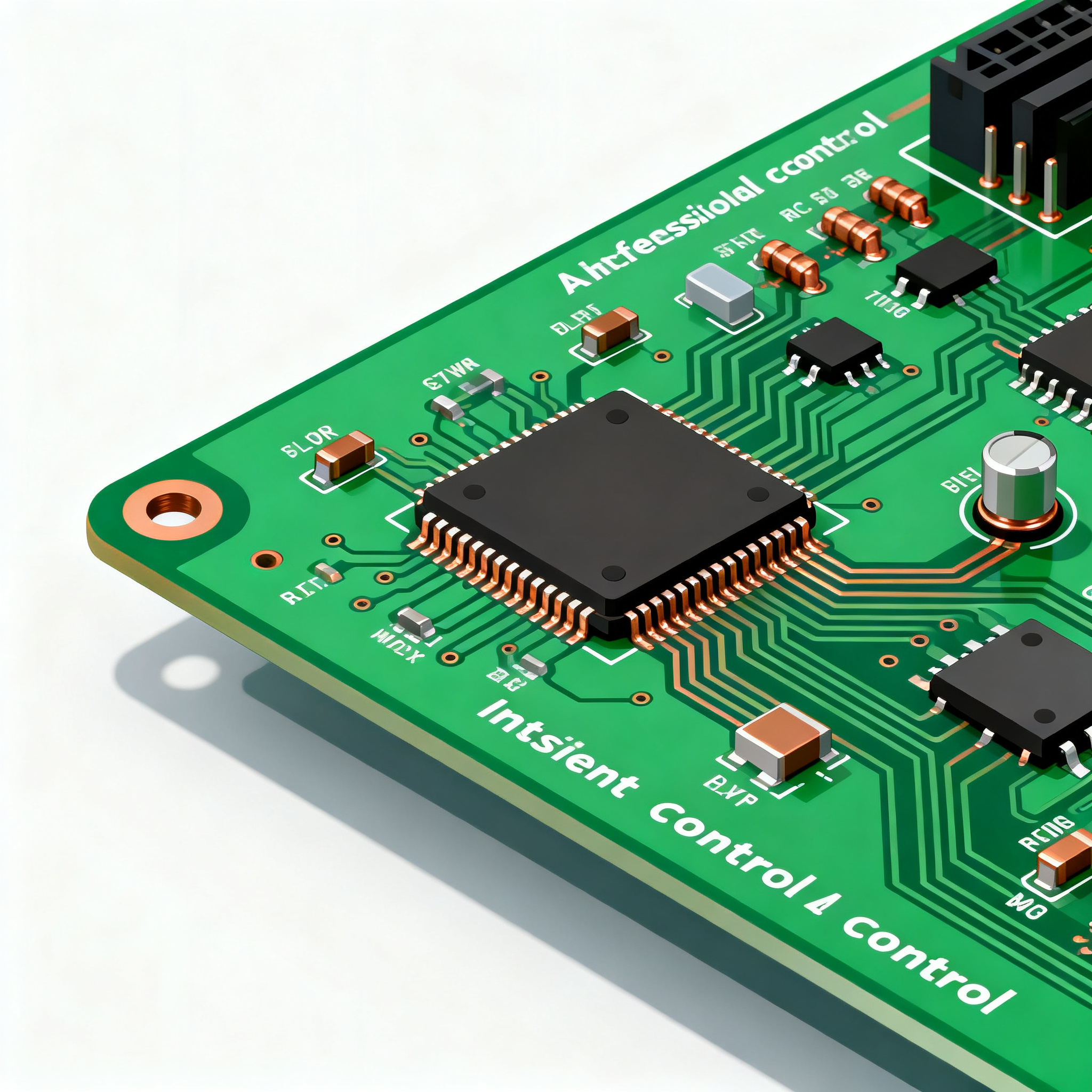
Engineer’s Field Guide to Security PCB Assembly: Selecting 4-Layer Impedance-Controlled Boards for Access Control Systems
Engineer’s Field Guide to Security PCB Assembly: Selecting 4‑Layer Impedance‑Controlled Boards for Access Control Systems The Failure Cases That Make 4‑Layer Impedance Control a Must for Access Contro...
Engineer’s Field Guide to Security PCB Assembly: Selecting 4‑Layer Impedance‑Controlled Boards for Access Control Systems
The Failure Cases That Make 4‑Layer Impedance Control a Must for Access Control PCB Assembly
When a card reader fails to authenticate or a door controller freezes during a security event, the root cause is often buried in the PCB stackup. Three recent failure cases illustrate why impedance‑controlled 4‑layer boards are non‑negotiable for access control hardware.
In a 4‑layer fine‑line engineering case, an ink‑filled via created an open circuit that went undetected until assembly. The CAM team flagged the issue because incorrect hole plating and solder mask bridging can escape electrical test. For a Wiegand reader or RS‑485 keypad, a single open via on a data line means intermittent badges or complete lock‑out—a security breach, not just a performance hiccup.
ESD damage is another silent killer. Matric’s failure analysis documents burnt components on boards assembled without proper ESD protocols. In access control, a latent ESD‑weakened transceiver can fail months later when a user touches the faceplate, leaving a door unsecured. The fix is not just a better design; it’s a contract manufacturer that uses ESD‑safe handling, anti‑static tools, and controlled environments as standard.
Stack‑up mismatches introduce impedance deviation and board warpage. A multilayer FR4 engineering query revealed that unconfirmed or mismatched prepregs led to registration errors and warpage severe enough to crack solder joints during thermal cycling. For outdoor gate controllers, this means moisture ingress and eventual failure of critical tamper‑detection circuits.
Security engineers also need to think like attackers. Reverse engineering analysis of PCBAs uses X‑ray imaging, delayering, and fault injection to expose vulnerabilities. A board with uncontrolled impedance radiates more electromagnetic noise, making differential power analysis or side‑channel attacks easier. Proper 4‑layer impedance control shrinks the attack surface by containing return currents and reducing unintended emissions.
The 4‑Layer Stackup Math That Locks in Signal Integrity for Access Control Hardware
Most access control peripherals—PoE door controllers, multi‑format readers, biometric terminals—rely on Ethernet, USB 2.0, or differential RS‑485. A 4‑layer SIG–GND–PWR–SIG stackup with high‑Tg FR4 gives every high‑speed signal a contiguous reference plane directly beneath it, providing a deterministic return path and tightly controlled impedance. Without that plane, return currents wander, creating crosstalk and ground bounce that can corrupt Wiegand data pulses or trigger false tamper alarms.
The stackup math begins with the dielectric constant (Dk) and thickness of the prepreg between the outer layer and the reference plane. Standard high‑Tg FR4 materials exhibit a Dk of about 4.2–4.5 at 1 GHz. Using a thinner prepreg allows a narrower trace for a given impedance, which saves routing space but demands tighter process control.
Table 1 shows three standard 4‑layer build‑ups commonly used for access control boards, derived from PCB Power’s impedance‑controlled build‑ups and NextPCB’s stackup design methodology. All assume 1 oz finished copper on outer layers and a 0.2 mm prepreg (≈1080) between L1‑L2 and L3‑L4, unless otherwise noted.
| Parameter | Build‑Up A (Standard 1.6 mm, 4‑layer) | Build‑Up B (Thin 1.0 mm, 4‑layer) | Build‑Up C (Thick 2.0 mm, 4‑layer) |
|---|---|---|---|
| Total board thickness | 1.6 mm | 1.0 mm | 2.0 mm |
| L1‑L2 prepreg | 1080 (0.077 mm Dk 4.2) | 1080 (0.077 mm Dk 4.2) | 2116 (0.12 mm Dk 4.3) |
| L2‑L3 core | 1.2 mm | 0.6 mm | 1.6 mm |
| L3‑L4 prepreg | 1080 (0.077 mm Dk 4.2) | 1080 (0.077 mm Dk 4.2) | 2116 (0.12 mm Dk 4.3) |
| 50Ω single‑ended trace width (L1/L4) | 0.15 mm (≈6 mil) | 0.12 mm (≈5 mil) | 0.20 mm (≈8 mil) |
| 90Ω differential pair width/spacing | 0.12/0.20 mm | 0.10/0.18 mm | 0.16/0.24 mm |
| 100Ω differential pair width/spacing | 0.10/0.25 mm | 0.09/0.22 mm | 0.14/0.30 mm |
| Typical process tolerance | ±10% | ±10% | ±10% |
| Suitable for | PoE door controllers, Ethernet readers | Compact mullion keypads, USB‑connected biometrics | High‑power gate controllers with heavy copper |
Key takeaway: If you maintain the same prepreg type (e.g., 1080) across projects, the trace width rules for 50Ω and 100Ω remain consistent regardless of total board thickness. This is the insight that NextPCB demonstrates—engineers can reuse proven geometries, speeding up design and reducing requalification. Always request the manufacturer’s actual dielectric constant for the batch of prepreg; a shift of Dk from 4.2 to 4.5 can change 50Ω trace width by 10–15%, pushing a design out of spec.
Standard vs. Custom Impedance Control: What Security PCB Buyers Are Really Paying For
When you order a 4‑layer impedance‑controlled board, you’re not just paying for FR4 and copper. You’re paying for the fabricator’s front‑end engineering and the certainty that your signals will behave as simulated. The market offers three distinct service tiers, each with different cost and reliability profiles.
Altium’s manufacturing guide stresses that clear fabrication notes are essential because different trace geometries on different layers may require different impedance values. A single impedance table in your fab drawing eliminates ambiguity. The table below compares the three typical approaches, factoring in insights from NextPCB, Wonderful PCB, and AdvancedPCB.
| Approach | Impedance Tolerance | Typical Cost Multiplier | Lead Time | Best for Security Applications |
|---|---|---|---|---|
| Fabricator’s standard stackup | ±10% | 1× (base) | Standard (5–10 days) | RS‑485 keypads, Wiegand readers, indoor access panels |
| Custom stackup with controlled Dk | ±5% | 1.3–1.6× | Standard + 1–2 days for engineering | Gigabit PoE door controllers, USB 2.0/3.0 biometric terminals |
| Rush impedance‑controlled service | ±10% or ±5% | 2–3× (Wonderful PCB data) | 1–4 days | Prototyping and trade‑show demos; not for cost‑sensitive production |
Hidden upcharges that affect final cost: AdvancedPCB notes that heavier copper (2 oz+), ENIG finish, and blind/buried vias each add cost. Fine‑pitch traces below 5 mil trigger a premium. Via‑in‑pad or sequential lamination for blind vias can double the board cost. Panel efficiency also matters: a poorly designed array with low utilization increases per‑board price. Always engage your PCB manufacturer during the layout phase to optimize panelization and avoid these surprises.
Decision flowchart in plain language:
– If your board has only RS‑485 or Wiegand signals and no PoE, a standard stackup with ±10% tolerance is sufficient.
– If you have Gigabit Ethernet, USB, or long differential pairs, specify ±5% tolerance and a custom stackup with documented Dk.
– If you need boards in 48 hours, rush service is available, but expect to pay 2–3× the standard price. Use it for prototypes only, and plan to requalify the design on standard lead time for production.
5 Impedance‑Control Pitfalls That Can Sink Your Security PCB Order
Even experienced engineers overlook details that cause batch rejection or field failures. The following five pitfalls are the most common we see in access control PCB designs, and each one is avoidable with a simple process change.
| Pitfall | Consequence | How to Avoid It |
|---|---|---|
| 1. Missing impedance table in fabrication notes | Fabricator guesses trace widths; impedance may be off by 20% | Use AllPCB’s impedance table guide to create a layer‑by‑layer table with target Z, trace width, spacing, and test frequency |
| 2. Ignoring solder mask effect on impedance | A 0.1 mil change in mask thickness can shift impedance by 2–3 Ω, enough to violate 100Ω specs | Ask the fabricator to include solder mask thickness in their field‑solver model; if you run your own simulations, add a 0.02 mm dielectric layer with Dk ≈ 3.5 on top of the traces |
| 3. Assuming all 1080 prepregs have the same Dk | Dk variation between material lots can shift impedance by 5–7 Ω | Request a material certificate for each batch; specify the exact prepreg type (e.g., Isola 1080 RC 54%) and confirm with FR4 spec sheets |
| 4. Overlooking test coupon requirements | Impedance measured on a coupon that doesn’t represent the actual board traces gives false confidence | Specify coupon layout, trace length, and measurement frequency (e.g., 100 MHz for Ethernet); require TDR report with each shipment |
| 5. Choosing via‑in‑pad or blind vias without cost analysis | Sequential lamination doubles the lamination cycles and can increase board cost by 50–100% | Use through‑hole vias wherever possible; if blind vias are unavoidable, consult AdvancedPCB’s cost guidance and discuss panel efficiency early |
Beyond these specifics, always verify the manufacturer’s proposed stackup before production. PCB Power’s standard build‑ups show that even a pre‑defined stackup should be confirmed with a cross‑section report and a test coupon. A reputable fabricator will provide a stack‑up drawing with nominal values; if they substitute a prepreg without your approval, reject the batch unless they prove the new dielectric constant yields the same impedance.
Security PCB Assembly Q&A: What Engineers and Buyers Ask Before Releasing a 4‑Layer Impedance‑Controlled Board
Q: Why can’t I just use a 2‑layer board for my access control reader? The data rates are only a few Mbps.
Even Wiegand and RS‑485 signals need a solid ground plane for consistent return paths. A 2‑layer board lacks a contiguous reference plane, causing EMI susceptibility and signal reflections that can trigger false reads or lock failures. A 4‑layer board provides the necessary impedance control and noise immunity, and it typically costs only 20–30% more than a 2‑layer board of the same size and thickness.
Q: What is the minimum impedance tolerance I should specify for a 4‑layer security board?
For most access control peripherals (keypads, Wiegand readers), ±10% is acceptable. If your board handles PoE Gigabit Ethernet or USB 2.0, specify ±5% to avoid signal degradation. For purely low‑speed RS‑485, ±10% is often sufficient, but tighter tolerances add negligible cost for the reliability gain. Always state the target impedance, tolerance, and test frequency in your fabrication notes.
Q: Do I need to specify ENIG finish for security boards?
ENIG (Electroless Nickel Immersion Gold) improves solderability and flatness for fine‑pitch components, reduces oxidation risk in outdoor readers, and ensures reliable edge‑connector contacts. For indoor keypads with coarser pitches, HASL (Hot Air Solder Leveling) can work, but ENIG is the safer choice for long‑term field reliability. The cost difference is typically 10–15% of the bare board price, a small premium for preventing corrosion‑related failures.
Q: How do I confirm the fabricator’s stackup before production?
Ask for a cross‑section report and impedance test coupon data. Verify that the prepreg material matches your specified dielectric constant and thickness. A reputable fabricator will provide a stack‑up drawing with nominal values before starting the run. If they substitute prepregs, reject the batch unless they prove the new dielectric constant yields the same impedance. This step is critical for security boards where long‑term reliability matters.
Q: What are the hidden costs when ordering 4‑layer impedance‑controlled boards?
Rush services can cost 2–3× standard lead time. Other hidden upcharges include fine‑pitch traces below 5 mil, heavy copper 2 oz+, via‑in‑pad or blind/buried vias (sequential lamination), and impedance test coupons. Panel utilization and array design also affect yield; maximizing panel efficiency reduces per‑board cost. Before finalizing your order, ask the fabricator to quote for both a standard and a high‑yield panel layout.
Q: Can I use a standard 4‑layer build‑up from a vendor like NextPCB or AdvancedPCB without a custom impedance design?
Yes, if your design’s trace widths and spacing match their pre‑defined stackup rules. Many vendors offer standard 4‑layer builds with 50Ω single‑ended and 90Ω/100Ω differential targets. Always request the exact stackup data and run a field solver simulation with the vendor’s dielectric constants to confirm impedance before releasing the order. This step takes minutes and can prevent a complete batch rejection.
From selecting the right stackup to specifying test coupons, every decision in your 4‑layer impedance‑controlled PCB order directly impacts the reliability of your access control system. At NovaPCBA, our assembly teams handle these boards daily, ensuring that every via, trace, and finish meets the stringent demands of security applications. Whether you’re prototyping a PoE door controller or ramping up production of multi‑format readers, we provide the process control and documentation you need to avoid field failures. Explore our security PCB assembly capabilities and let us help you lock in signal integrity from the first prototype.
References & Further Reading
- 4‑Layer Fine‑Line PCB Engineering Case: Impedance Control, Copper Thickness & Solder Mask Bridge Challenges
- 6 Common Causes of PCB Failure: What OEMs Should Know
- Multilayer FR4 PCB Engineering Queries Explained: Causes, Risks and Solutions
- Reverse Engineering PCBA: Assessing Reliability and Identifying Vulnerabilities
- 4‑Layer PCB Stackup Design and Impedance Control | NextPCB
- 4‑Layer PCB Manufacturing and Stack‑up – Wonderful PCB
- Improving Signal Integrity with 4 Layer PCB Technology | AdvancedPCB
- Impedance Control: How to Specify Your Requirements for PCB Manufacturers | Altium
- FR4 PCB Material Specification Sheet (PDF) | 2026 Technical Selection Guide
- How to Specify Impedance Control Requirements to Your PCB Manufacturer
- Impedance Controlled Standard Build‑ups | PCB Power