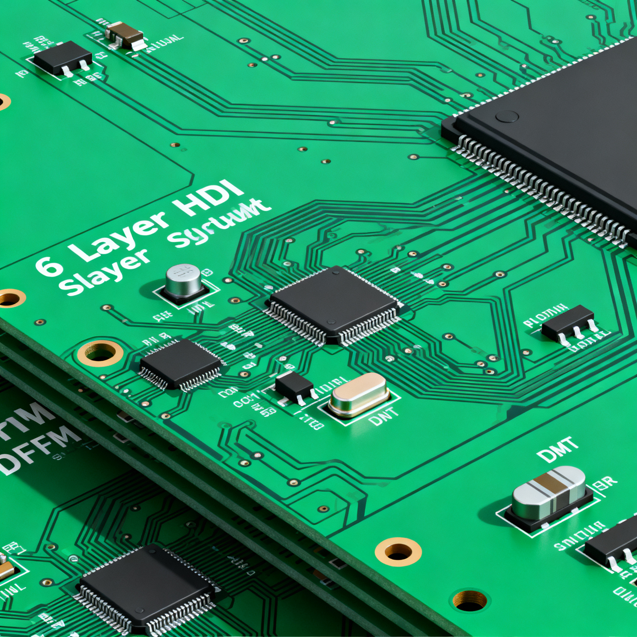
Engineer’s Field Guide to Consumer Electronics PCB Assembly: High-Volume SMT, DFM, and 6-Layer HDI Stackups
When a $0.03 Capacitor Triggers a Consumer Electronics Recall: Why High-Volume SMT Demands DFM Rigor It starts with a single 0201 MLCC—costing less than three cents—that tombstoned during reflow. The ...
When a $0.03 Capacitor Triggers a Consumer Electronics Recall: Why High-Volume SMT Demands DFM Rigor
It starts with a single 0201 MLCC—costing less than three cents—that tombstoned during reflow. The board passed electrical test because the capacitor’s termination still made marginal contact, but after six months in the field, thermal cycling and vibration opened the joint. The result: intermittent Wi‑Fi dropouts on a smart home hub that had already shipped 200,000 units. The brand’s recall, tracked in the CPSC consumer electronics recall database, stopped shipments, consumed engineering and legal staff for weeks, and created a component shortage ripple across three other SKUs that shared the same capacitor. As the EE Times recall management guide warns, a recall can stop shipments, delay production, create shortages, tie up staff, and interfere with normal order fulfillment. In consumer electronics, where identical passives are reused across product families, one DFM oversight becomes a business crisis.
Component misalignment and tombstoning are among the most common SMT defects, as documented in AllPCB’s defect troubleshooting guide: components placed incorrectly on the PCB, leading to poor connections. When you multiply that risk by millions of placements per day on a high‑volume line, the probability of a latent field failure is not negligible—it’s inevitable without rigorous DFM and process control. This is why burn‑in testing, though it adds moderate upfront cost, avoids substantial follow‑up losses including product returns, warranty compensation, on‑site maintenance, and batch product recalls, as PCBCart’s burn‑in economics analysis makes clear. For an engineer or buyer scaling a consumer product from prototype to mass production, the lesson is blunt: every cent saved by skipping DFM review or test coverage is a future recall liability.
Inside a 6-Layer HDI Stackup: Via Structures, Impedance Control, and Material Choices for Mass Production
Consumer wearables, hearables, and compact IoT hubs routinely demand 6‑layer HDI boards that squeeze high‑speed digital, RF, and power delivery into a 0.8‑mm or 1.0‑mm total thickness. The stackup you choose directly determines manufacturability, signal integrity, and drop‑test survival. Most designs adopt a 1+N+1 structure (one microvia layer on each side, with a 4‑layer core) or a 2+N+2 structure when routing density requires stacked or staggered microvias. The table below captures the key parameters you’ll negotiate with your fab and assembly partner.
| Parameter | Typical 1+N+1 6‑Layer HDI | 2+N+2 6‑Layer HDI | Selection Notes |
|---|---|---|---|
| Total thickness | 0.8 – 1.0 mm | 0.8 – 1.2 mm | Thinner improves Z‑axis reliability in drop tests; thicker aids impedance control. |
| Layer stack | L1 (microvia) – L2 (buried) – L3–L4 core – L5 (buried) – L6 (microvia) | L1–L2 microvia, L2–L5 buried, L5–L6 microvia (stacked or staggered) | 1+N+1 is lower cost and risk; 2+N+2 needed for dense BGA breakouts. |
| Microvia diameter / capture pad | 0.1 mm / 0.25 mm | 0.1 mm / 0.25 mm (stacked vias may require larger capture) | Follow IPC‑6012 class 2 or 3 for annular ring requirements. |
| Dielectric material | High‑Tg FR‑4 (Tg ≥ 170°C) | High‑Tg FR‑4 or mid‑loss (e.g., Nelco N4000‑13) | Refer to ApolloPCB’s FR4 material specification sheet for Tg, CTE, and Td data. |
| Trace / space (outer) | 75 / 75 µm (3/3 mil) | 60 / 60 µm (2.4/2.4 mil) | Tighter L/S increases cost; verify fab capability before committing. |
| Impedance control tolerance | ±10% (single‑ended 50 Ω, diff. 90 Ω or 100 Ω) | ±10% (may require ±7% for USB 3.x / PCIe) | Use polar or field solver; confirm with fab’s stackup calculator. |
| Copper thickness (outer/inner) | 35 µm / 35 µm (1 oz) | 35 µm / 35 µm (1 oz); power layers may use 70 µm (2 oz) | Thicker copper helps IR drop but complicates etching fine lines. |
| Solder mask registration | ±50 µm | ±50 µm | Critical for 0.4 mm pitch BGAs; LPI mask preferred. |
Material selection is not just about Tg. The CTE mismatch between the laminate and copper must stay within limits that prevent barrel cracking during reflow and thermal cycling. For consumer products that experience daily temperature swings, a Tg of 170°C or higher with a low Z‑axis CTE (below 3.5% at 50–260°C) is the baseline. The ApolloPCB FR4 specification sheet provides the Td and CTE curves you need to compare laminates.
Once the board is fabricated, assembly acceptance criteria must align with high‑volume consumer expectations. Wevolver’s SMT guide highlights that IPC‑A‑610 provides visual criteria and guidelines for acceptable solder joint, component placement, and overall workmanship for assembled PCBs. Meanwhile, PCBCool’s SMT process flow references IPC J‑STD‑001J (Requirements for Soldered Electrical and Electronic Assemblies) as the process standard. Together, these standards define the solder fillet shape, voiding limits, and microvia fill requirements that keep a 6‑layer HDI board reliable over a 2‑year consumer warranty window.
SMT vs. Through-Hole and EMS vs. SMT-Only: Matching Assembly Strategy to Production Volume
Consumer electronics teams often face a fork in the road: commit to a full‑SMT design that eliminates wave soldering, or retain a few through‑hole connectors for mechanical robustness. The decision hinges on annual volume, product lifecycle, and the cost of engineering changes. The table below compares the three most common assembly strategies for consumer products.
| Metric | Full SMT | Mixed Technology (SMT + Through‑Hole) | Through‑Hole Dominant | Selection Criteria & Failure Boundary |
|---|---|---|---|---|
| Typical annual volume | ≥10,000 units | 5,000 – 50,000 units | <5,000 units (prototype/niche) | Below 5k, through‑hole NRE is lower; above 10k, SMT automation dominates. |
| Unit assembly cost (relative) | Lowest at scale | Medium (wave solder adds cost) | Highest (manual labor) | AllPCB’s cost analysis confirms SMT assembly cost is generally lower for high‑volume production due to automation and smaller component sizes. |
| NRE investment | Moderate (stencil, pick‑and‑place programming) | Higher (stencil + wave pallet + selective solder fixtures) | Low (manual assembly tooling) | NRE amortized over volume; for 12‑24 month lifecycle, SMT NRE is negligible per board. |
| Component density | Very high (0201, 0.4 mm pitch BGA) | High on SMT side; through‑hole connectors on edges | Low; board area dominated by leaded parts | Density drives PCB layer count and HDI requirement. |
| Lead time (typical) | 2–4 weeks turnkey | 3–5 weeks | 4–6 weeks (manual assembly) | Turnkey EMS can parallelize fab and kitting, shaving 1–2 weeks off total lead time. |
| Reliability concerns | Tombstoning, head‑in‑pillow, microvia cracks | Through‑hole barrel fatigue, wave solder bridging | Hand‑soldering consistency, flux residues | Consumer drop‑test and thermal cycling requirements favor SMT with proper DFM. |
Beyond the assembly technology, you must also decide between a turnkey EMS partner and managing PCB fabrication and SMT assembly separately. GNSEMS’s comparison of EMS vs. SMT‑only factories notes that for consumer electronics with a stable 12–24 month lifecycle and confirmed component qualification, a turnkey EMS reduces logistics handoffs and often lowers landed cost—even if the unit price appears higher—because it eliminates separate fab lead time, kitting, and subcontracting overhead. Conversely, if your product undergoes frequent engineering changes, managing fab and assembly separately can give you more control, but you’ll pay for it in coordination time and risk of component shortages. Topfastpcb’s consumer electronics factory overview reinforces that automated production workflows and supply chain coordination are essential for stable quality at scale.
Tip: If your BOM contains a mix of 0201 passives and a few high‑retention USB‑C or audio jacks, consider a full‑SMT design with surface‑mount versions of those connectors. Modern SMT USB‑C receptacles with through‑hole shell stakes can be reflow‑soldered without wave solder, preserving the cost advantage of a single‑side SMT line. This eliminates the mixed‑technology penalty while maintaining mechanical strength.
DFM Traps That Kill Yield in Consumer Electronics: Footprint Design, Panelization, and Test Access
High‑volume SMT lines run at placement speeds exceeding 40,000 components per hour. At that cadence, a footprint that violates IPC‑7351 courtyard rules or a panel that flexes during depaneling will generate defects faster than AOI can catch them. The following table maps the most common DFM traps to their root causes and proven fixes.
| DFM Trap | Root Cause | Field Consequence | Fix & Reference |
|---|---|---|---|
| Tombstoning on 0201/0402 passives | Unequal thermal mass on pads, asymmetric solder paste volume, or pad size mismatch | Intermittent open circuits; latent field failures | Match pad dimensions to IPC‑7351 land patterns; balance copper thermal relief; keep stencil thickness ≤0.1 mm for 0201. |
| Component misalignment / skew | Insufficient fiducial count, poor panel rigidity, or placement force variation | Shorts or opens, especially on fine‑pitch QFNs and BGAs | Use three global fiducials plus local fiducials for 0.5 mm pitch and below; follow AllPCB’s misalignment troubleshooting. |
| Solder bridging on 0.4 mm pitch BGAs | Excessive solder paste, poor stencil design, or inadequate reflow profile | Short circuits that may pass cold‑test but fail under thermal stress | Use laser‑cut stencil with 80 µm thickness, type 4 or 5 solder paste, and nitrogen reflow for fine pitch. |
| Insufficient test access | No test points on critical nets; vias not tented or filled | Unable to perform ICT or flying‑probe test; escapes rise | Add 1.0 mm diameter test pads on all power rails and critical signals; tent unused vias to prevent solder wicking. |
| Panel bow and twist during reflow | Unbalanced copper distribution, thin core, or excessive panel size | Misregistration, tombstoning, and BGA non‑wets | Target 80–85% panel utilization on 18″×24″ standard panel; add 10–15 mm edge rails with tooling holes and fiducials; balance copper on outer layers. |
Panelization economics directly impact per‑board cost. For a 50 × 30 mm consumer PCB, you can fit approximately 120–140 boards on an 18″×24″ panel at 80% utilization. Dropping to 70% utilization increases the per‑board substrate cost by 14–20%, which on a million‑unit run becomes a six‑figure penalty. But pushing utilization above 85% often compromises depaneling clearance and increases flex, leading to higher defect rates. The PCB Power footprint guide emphasizes that courtyard rules must account for depaneling tolerances—rout or V‑score keep‑out zones should never encroach on component bodies.
Test strategy is the other half of the DFM equation. In‑circuit test (ICT) fixtures are expensive but provide fast, comprehensive coverage for high‑volume runs. Flying‑probe testers avoid fixture NRE and are ideal for mid‑volume or products with frequent revisions. Regardless of the method, you must design test access from day one. A common mistake is to omit test points on DDR memory interfaces or PMIC outputs, assuming boundary scan will cover them. Boundary scan cannot detect a missing decoupling capacitor or a cold solder joint on a power FET. When infant mortality risks are high—for example, in always‑on IoT hubs that have no user‑serviceable parts—adding burn‑in testing is a cost‑effective insurance policy. PCBCart’s analysis shows that burn‑in avoids recall and on‑site maintenance expenses that can exceed the test cost by an order of magnitude.
Consumer Electronics PCB Assembly: Questions from the Production Floor
Q: At what annual volume does switching from through‑hole to full SMT become cost‑justified for a consumer product?
Typically above 5,000–10,000 units per year, SMT’s automation and smaller component costs outweigh through‑hole’s lower NRE. The exact crossover depends on board complexity, connector mix, and whether wave soldering can be eliminated. AllPCB’s cost analysis confirms that SMT assembly cost is generally lower for high‑volume production, while GNSEMS’s EMS vs. SMT‑only comparison shows that for stable 12–24 month lifecycle products, turnkey SMT often yields lower landed cost even at moderate volumes. If your design still needs a few through‑hole connectors, evaluate surface‑mount alternatives before committing to a mixed‑technology line.
Q: How do I qualify a 6‑layer HDI stackup for drop‑test reliability in wearables?
Start with a 1+N+1 stackup using microvias on outer layers and a high‑Tg FR‑4 (≥170°C). Validate with IST (interconnect stress testing) and drop simulations per JEDEC JESD22‑B111, then correlate with actual product‑level drop tests on assembled units. ApolloPCB’s material specs provide the Tg, CTE, and Td data needed to select a laminate that won’t delaminate under shock. Wevolver’s IPC‑A‑610 workmanship criteria give you the acceptance benchmarks for solder joint integrity after drop testing.
Q: What panel utilization rate should I target for a 50 × 30 mm consumer PCB to minimize cost?
Aim for 80–85% utilization on a standard 18″ × 24″ panel. Include 10–15 mm edge rails for tooling, fiducials, and test coupons. Lower utilization drives up per‑board cost; higher may compromise depaneling and increase flex, leading to tombstoning and BGA defects. The PCB Power footprint guide provides courtyard rules that help you maintain safe clearances between board outlines and components for V‑score or rout depaneling.
Q: When is it worth paying for burn‑in testing on consumer IoT boards?
Burn‑in is justified when infant mortality failures could trigger a recall or high warranty costs—typically for products with always‑on power, safety functions, or no user‑serviceable parts. PCBCart’s analysis shows that burn‑in avoids recall and on‑site maintenance expenses that dwarf the upfront test cost. For a smart thermostat or a connected smoke alarm, a 24‑hour powered burn‑in at elevated temperature can screen out weak solder joints and marginal components before they reach the consumer.
Q: How do I avoid tombstoning on 0201 passives during high‑speed placement?
Match pad size and shape to IPC‑7351 recommendations, balance thermal relief on both pads, and keep solder paste volume consistent with stencil thickness ≤0.1 mm. AllPCB’s defect guide highlights misalignment and uneven wetting as root causes; proper DFM and solder paste inspection (SPI) are the fix. Also ensure your pick‑and‑place machine’s placement force is calibrated for 0201 components—excessive force can skew the part before reflow.
Q: What’s the real lead time difference between a turnkey EMS and managing PCB fab and assembly separately?
A turnkey EMS typically shaves 1–2 weeks off total lead time by parallelizing fab, component kitting, and assembly. Managing separately adds logistics handoffs and risks component shortages. GNSEMS’s comparison notes that for stable 12–24 month lifecycle products, turnkey often lowers landed cost despite higher unit price, because you avoid the hidden costs of expediting, multiple supplier margins, and re‑kitting delays. If your product is still in engineering validation, however, a separate fab and assembly approach may give you the flexibility to change laminate or surface finish without re‑negotiating a full turnkey contract.
Scaling a consumer electronics PCB from prototype to millions of units demands that every design decision—stackup, footprint, panelization, test access—be evaluated through the lens of high‑volume SMT yield. At NovaPCBA, we support engineers and buyers with turnkey PCBA services that integrate HDI fabrication, precision SMT assembly, and DFM feedback early in the design cycle. By applying the field‑tested principles in this guide, you can avoid the $0.03 capacitor trap and deliver products that perform reliably from the first unit to the last.
References & Further Reading
- Product Recall Management for Electronics Manufacturing SMBs – EE Times
- Electronics Recalls – CPSC.gov
- Burn‑In Testing: Filtering Out Infant Mortality – PCBCart
- SMT Assembly Defects: The Ultimate Troubleshooting Guide – AllPCB
- SMT vs. Through Hole: A Cost Analysis Showdown – AllPCB
- Surface‑mount technology – Wikipedia
- How to Choose Between EMS vs SMT Factory – GNSEMS
- Consumer Electronics PCB Factory: Speed, Cost, and Mass Production – Topfastpcb
- SMT PCB Assembly: A Comprehensive Guide – Wevolver
- SMT Footprint Guide: IPC‑7351 Land Patterns – PCB Power
- FR4 PCB Material Specification Sheet – ApolloPCB
- SMT Assembly Process Flow for PCBA Manufacturing – PCBCool