Effective Strategies for PCB Assembly Cost Reduction: Real-World Examples That Work
Effective Strategies for PCB Assembly Cost Reduction Introduction In the competitive world of electronics manufacturing, reducing costs without sacrificing quality is crucial. Printed Circuit Board (P...
Introduction
In the competitive world of electronics manufacturing, reducing costs without sacrificing quality is crucial. Printed Circuit Board (PCB) assembly can be a significant portion of the production expense. Effective strategies for cost reduction in PCB assembly are therefore essential. This article explores practical methods to minimize costs through optimized PCB design, layout rules, stackup design, and careful choice of materials, all while maintaining signal integrity and meeting manufacturing requirements.
Technical Overview
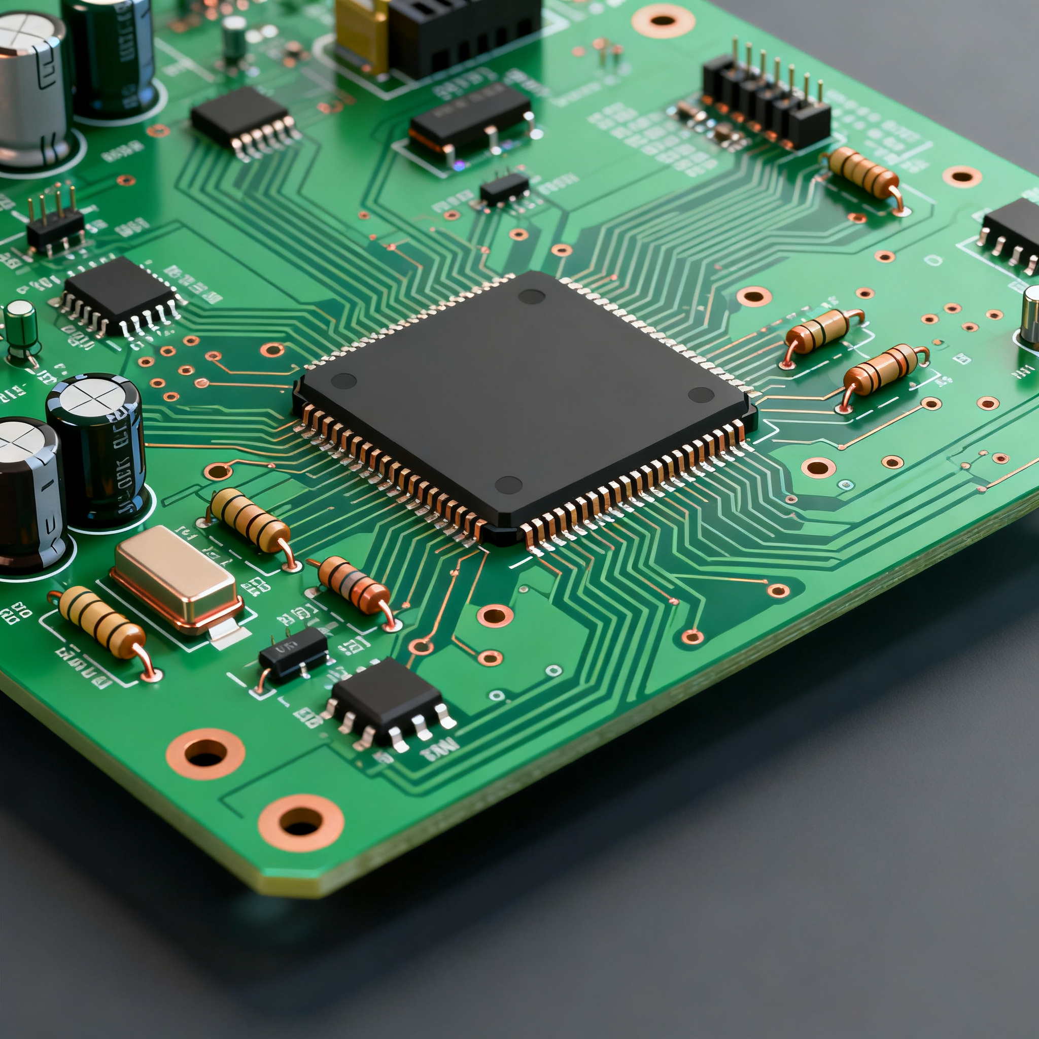
Understanding the core concepts of PCB design is pivotal in reducing assembly costs. The architecture of a PCB involves multiple layers, each serving specific functions. The design principles include ensuring proper trace width, spacing, and via sizes, which are critical for signal integrity and manufacturability. Adhering to industry standards like IPC-2221 and IPC-A-610 ensures quality and reliability. Additionally, the selection of materials such as FR-4 or Rogers, which vary in dielectric properties, impacts both performance and cost. By optimizing these factors, significant cost savings can be achieved in the manufacturing process.
Detailed Specifications
Specifications are the backbone of PCB design, dictating how the board will perform and how much it will cost to produce. Key specifications include trace width, spacing, via sizes, and clearances. These factors influence the signal integrity, thermal management, and manufacturability of the PCB. Below is a detailed table outlining essential PCB design rules.
| Design Parameter | Minimum Value | Recommended Value |
|---|---|---|
| Trace Width | 4 mils | 6 mils |
| Trace Spacing | 4 mils | 8 mils |
| Via Diameter | 8 mils | 10 mils |
| Via Hole Size | 4 mils | 6 mils |
| Annular Ring | 4 mils | 6 mils |
| Pad-to-Trace Clearance | 4 mils | 8 mils |
| Board Edge Clearance | 10 mils | 20 mils |
| Silkscreen Text Height | 30 mils | 40 mils |
| Silkscreen Text Width | 5 mils | 6 mils |
| Solder Mask Clearance | 4 mils | 6 mils |
| Solder Mask Dam | 4 mils | 5 mils |
Key Takeaways from the Specifications
The specifications outlined in the table above are essential for ensuring both the performance and manufacturability of a PCB. Trace width and spacing are especially critical for maintaining signal integrity and preventing short circuits. Adequate via sizes and clearances are necessary for reliable electrical connections and thermal management. By adhering to these guidelines, designers can minimize the risk of defects and reduce the overall cost of PCB assembly. These specifications also facilitate compliance with IPC standards, ensuring quality and consistency in production.
| Layer Configuration | Description | Applications |
|---|---|---|
| 2-Layer | Basic configuration with top and bottom layers | Simple consumer electronics |
| 4-Layer | Includes power and ground planes | Complex consumer electronics |
| 6-Layer | Two additional signal layers | High-speed applications |
| 8-Layer | Enhanced signal integrity with additional planes | Advanced computing |
| 10-Layer | High-density interconnects | Telecommunications |
| 12-Layer | Maximum signal routing capacity | Aerospace and defense |
Practical Implications
The choice of layer stackup significantly influences the performance and cost of a PCB. A 2-layer board is cost-effective for simple designs, while more complex applications may require 4 or more layers to accommodate additional signal routing and power distribution. Higher layer counts, such as 8 or 10, enhance signal integrity and are suitable for high-speed or high-density applications. Understanding these configurations helps in selecting the appropriate stackup for specific applications, balancing performance requirements with cost constraints.
| Material | Dielectric Constant (εr) | Loss Tangent |
|---|---|---|
| FR-4 | 4.5 | 0.02 |
| Rogers 4350B | 3.48 | 0.0037 |
| Rogers 4003C | 3.55 | 0.0027 |
| Isola FR408 | 3.75 | 0.009 |
| Nelco N4000-13 | 3.7 | 0.009 |
| Arlon 85N | 3.5 | 0.004 |
| Polyimide | 4.2 | 0.004 |
| PTFE | 2.1 | 0.001 |
Application Guidelines
Selecting the right material is crucial for both performance and cost management in PCB design. FR-4 is a popular choice due to its balance of cost and performance, suitable for a wide range of applications. For high-frequency applications, materials like Rogers 4350B and PTFE offer lower dielectric constants and loss tangents, which are essential for minimizing signal loss. Understanding the material properties helps in choosing the right substrate for specific needs, optimizing both performance and budget.
Design Considerations
When designing a PCB, several factors must be taken into account to ensure cost-effective production and high performance. The choice of design rules, such as trace width and spacing, directly impacts manufacturability and yield. Stackup design is another critical consideration; it affects signal integrity and the ability to manage power distribution effectively. Material selection also plays a vital role, as it influences dielectric properties and thermal performance. By carefully considering these elements, designers can create PCB layouts that are both efficient and cost-effective.
Step-by-Step Implementation
- Define Requirements: Start by outlining the electrical and mechanical requirements for your PCB. This includes the number of layers, signal integrity needs, and thermal considerations.
- Choose Materials: Select appropriate materials based on performance and cost. Consider factors like dielectric constant and loss tangent for high-frequency applications.
- Design the Stackup: Determine the optimal layer configuration to balance performance and cost. More layers may be necessary for complex designs.
- Set Design Rules: Establish trace widths, spacings, and via sizes based on manufacturing capabilities and performance requirements.
- Layout the PCB: Use CAD software to layout the PCB, adhering to the established design rules and stackup configuration.
- Simulate Signal Integrity: Perform simulations to ensure that the design meets signal integrity requirements, making adjustments as necessary.
- Review and Revise: Conduct a thorough review of the design, checking for manufacturability and potential issues.
- Finalize Documentation: Prepare detailed documentation for manufacturing, including Gerber files and a Bill of Materials (BOM).
Common Issues & Solutions
- Signal Integrity Problems: Use proper trace width and spacing to minimize crosstalk and ensure signal integrity.
- Thermal Management Issues: Implement thermal vias and heat sinks to dissipate heat effectively.
- Manufacturability Concerns: Adhere to standard design rules to ensure ease of production and high yield.
- Material Cost Overruns: Choose materials that provide the necessary performance at the lowest cost.
- Layer Misalignment: Ensure precise alignment in the stackup design to avoid connectivity issues.
- Impedance Matching Errors: Use controlled impedance traces for high-speed signals to prevent signal degradation.
Applications & Use Cases
PCBs are used in a wide range of applications, from simple consumer electronics to complex aerospace systems. In consumer electronics, cost-effective 2-layer boards are common, while telecommunications and computing often require multi-layer boards for enhanced performance. In aerospace and defense, high-reliability PCBs with advanced materials are used to withstand harsh environments. By understanding the specific requirements of each application, designers can select the appropriate PCB configuration to meet both performance and cost objectives.
Selection & Sourcing Guide
Choosing the right components and materials is critical for effective PCB design. For sourcing, consider using platforms like IC Online, which offers a wide range of electronic components, ensuring both quality and competitive pricing. Evaluate suppliers based on their capabilities, lead times, and adherence to industry standards.
FAQ
- What is the most cost-effective material for PCBs? FR-4 is commonly used due to its balance of cost and performance.
- How do I choose the right layer stackup? Consider the complexity of your design and signal integrity requirements; use more layers for complex, high-speed applications.
- What is the importance of trace width? Proper trace width ensures signal integrity and prevents overheating.
- How can I reduce PCB assembly costs? Optimize design rules, select cost-effective materials, and choose an efficient stackup configuration.
- What are IPC standards? IPC standards ensure quality and reliability in PCB design and manufacturing.
- How does dielectric constant affect PCB design? It influences signal speed and impedance; lower values are better for high-frequency applications.
- What is the role of a solder mask? It protects the PCB from oxidation and prevents solder bridges.
- Can I use a single-layer PCB for complex designs? Single-layer PCBs are limited in complexity and are not suitable for advanced applications.
- How do I ensure signal integrity? Use proper design rules, simulate the design, and select appropriate materials.
- What is a Gerber file? A Gerber file is a standard file format for PCB manufacturing, detailing the layout and design.
Conclusion
Effective PCB assembly cost reduction requires a strategic approach to design, material selection, and manufacturing processes. By adhering to design rules, optimizing layer stackups, and selecting appropriate materials, significant cost savings can be achieved without compromising quality. Understanding these elements and their implications in real-world applications is key to successful PCB design and production.