Designing PCB Layouts for EMI Compliance: Step-by-Step Techniques for Optimal Results
Designing PCB Layouts for EMI Compliance Introduction In today's electronics landscape, ensuring Electromagnetic Interference (EMI) compliance is crucial for the reliability and performance of electro...
Introduction
In today's electronics landscape, ensuring Electromagnetic Interference (EMI) compliance is crucial for the reliability and performance of electronic devices. EMI can disrupt the normal operation of circuits, leading to performance degradation and regulatory non-compliance. As electronics become more compact and complex, designing Printed Circuit Boards (PCBs) that mitigate EMI issues is more important than ever. This article delves into the intricacies of designing PCB layouts for EMI compliance, focusing on circuit topology, component calculations, performance analysis, and design trade-offs.
Technical Overview
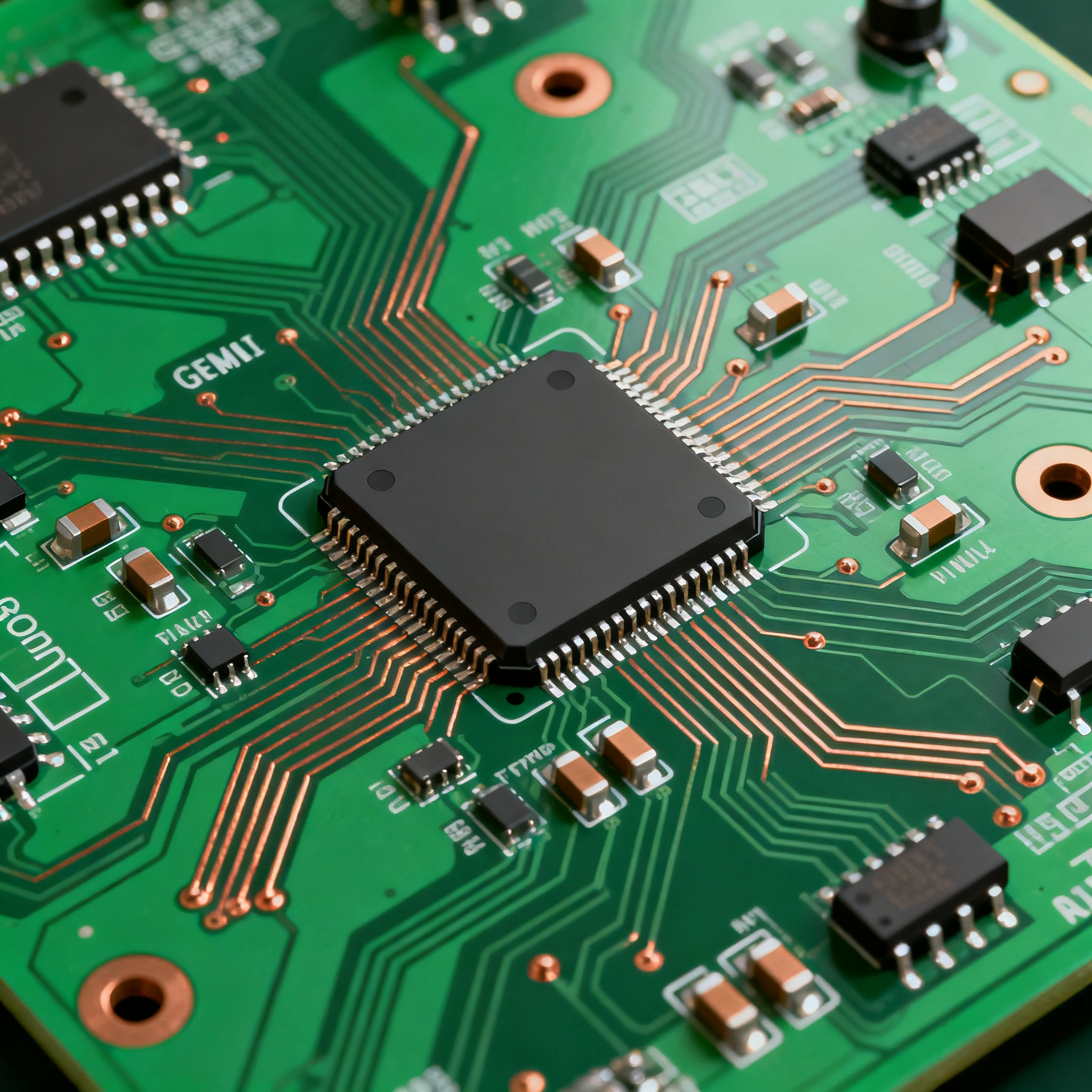
To achieve EMI compliance in PCB designs, engineers must consider several core concepts and architectural principles. The primary focus is on minimizing electromagnetic emissions and susceptibility through strategic component placement, trace routing, and layer stackup. Key architectural principles include:
- Ground Plane Design: Implementing a contiguous ground plane to reduce loop areas and provide a low-impedance return path for signals.
- Signal Integrity: Ensuring signal traces are short and direct to minimize inductive and capacitive coupling.
- Shielding: Using shielding techniques to isolate sensitive components from potential EMI sources.
These principles help mitigate EMI by controlling the electromagnetic fields generated by the circuit, thus ensuring compliance with industry standards such as those outlined by the IPC.
Detailed Specifications
Understanding the detailed specifications of your PCB design is critical for EMI compliance. These specifications guide the selection of component values, the calculation of electrical parameters, and the overall circuit topology. Below is a table showcasing essential design parameters that influence EMI performance.
| Parameter | Value/Formula | Description |
|---|---|---|
| Resistor (R1) | 10kΩ | Limits current to prevent circuit overload |
| Capacitor (C1) | 100nF | Decoupling capacitor for noise reduction |
| Inductor (L1) | 1μH | Used for filtering high-frequency noise |
| Trace Width | 0.25mm | Ensures proper current handling and EMI reduction |
| Layer Stackup | 4-layer | Improves signal integrity and EMI shielding |
| Via Count | 20 | Minimizes inductive effects by reducing loop area |
| Ground Plane | Continuous | Reduces EMI by providing a common return path |
| Signal Trace Length | <10cm | Short trace length to minimize inductive coupling |
| Component Placement | Compact | Reduces loop areas and potential EMI sources |
| Shielding Material | Aluminum | Used to shield sensitive areas from EMI |
Key Takeaways from the Specifications
The design parameters table highlights critical specifications that influence EMI compliance. For instance, using a continuous ground plane and ensuring short signal trace lengths are fundamental practices to minimize electromagnetic emissions. The choice of a 4-layer stackup enhances signal integrity, while decoupling capacitors like C1 (100nF) play a vital role in noise reduction. These parameters should be carefully calculated and adjusted to meet specific design requirements, ensuring optimal performance and compliance with industry standards.
| Performance Metric | Value | Impact on Design |
|---|---|---|
| Gain | 20dB | Amplifies signal while maintaining low noise |
| Bandwidth | 2MHz | Determines the range of frequencies the circuit can handle |
| Signal-to-Noise Ratio (SNR) | 60dB | Ensures clear signal transmission |
| Power Consumption | 500mW | Influences thermal management and efficiency |
| Harmonic Distortion | 0.02% | Low distortion indicates high signal fidelity |
| Rise Time | 10ns | Affects the speed of signal transitions |
| Crosstalk | −30dB | Measures unwanted coupling between traces |
| Input Impedance | 50Ω | Matches source impedance for maximum power transfer |
Practical Implications
The performance analysis table provides insights into how various metrics affect the overall design. For example, a high gain of 20dB is beneficial for amplifying signals, but it must be balanced with low harmonic distortion (0.02%) to maintain signal fidelity. The bandwidth of 2MHz ensures the circuit can handle a wide range of frequencies, while a signal-to-noise ratio of 60dB is crucial for clear signal transmission. These metrics must be optimized according to the specific application requirements to achieve the desired performance while maintaining EMI compliance.
| Configuration | Pros | Cons |
|---|---|---|
| Single-Layer PCB | Cost-effective, simple design | Limited routing space, poor EMI performance |
| Double-Layer PCB | Improved routing options, moderate cost | Still limited EMI shielding compared to multi-layer PCBs |
| Multi-Layer PCB | Excellent EMI performance, compact design | Higher cost, complex manufacturing |
| Microstrip Layout | High-frequency performance, reduced crosstalk | Complexity in design and manufacturing |
| Stripline Layout | Superior EMI shielding, reduced emissions | Requires precise layer stackup, increased cost |
| Embedded Components | Space-saving, reduced parasitics | Complex assembly, higher cost |
Application Guidelines
The design trade-offs table illustrates the pros and cons of various PCB configurations. While single-layer PCBs are cost-effective, they offer limited EMI performance. In contrast, multi-layer PCBs provide excellent EMI shielding but at a higher cost. Microstrip and stripline layouts are ideal for high-frequency applications, offering reduced crosstalk and emissions. Selecting the right configuration depends on the specific requirements, budget, and intended application. Understanding these trade-offs is essential for making informed design decisions that balance performance, cost, and manufacturability.
Design Considerations
Designing PCBs for EMI compliance involves several practical considerations that influence both the performance and manufacturability of the final product. Here are some key design guidelines to follow:
- Component Placement: Place components to minimize loop areas. Critical components should be placed close to their corresponding connectors to reduce trace lengths and potential EMI sources.
- Trace Routing: Keep signal traces short and direct. Avoid 90-degree bends which can increase inductive and capacitive coupling. Use vias judiciously to minimize inductive effects.
- Ground Plane Management: Implement a continuous ground plane for a low-impedance return path. This reduces the potential for EMI by minimizing loop areas and providing effective shielding.
- Decoupling Capacitors: Use decoupling capacitors near power pins of ICs to filter out high-frequency noise. This helps maintain signal integrity and reduces potential EMI.
- Layer Stackup: Consider using a multi-layer stackup to improve EMI performance. This provides additional routing options, better signal integrity, and effective shielding.
- Shielding Techniques: Utilize shielding materials like aluminum or copper to isolate sensitive components from potential EMI sources. This is particularly important in high-frequency applications.
By following these design guidelines, engineers can effectively mitigate EMI issues and ensure compliance with industry standards, resulting in reliable and high-performance PCB designs.
Step-by-Step Implementation
Implementing a PCB design for EMI compliance involves a series of detailed steps to ensure optimal results. Here is a step-by-step guide:
- Define Design Requirements: Clearly outline the performance, cost, and compliance requirements for your PCB design.
- Select Appropriate Components: Choose components that meet the design specifications and EMI requirements. Consider factors such as package size, power consumption, and frequency response.
- Plan the Layer Stackup: Determine the number of layers required for your design. A multi-layer stackup is recommended for improved EMI performance.
- Place Components Strategically: Position components to minimize trace lengths and loop areas. Ensure critical components are placed close to their connectors.
- Route Traces Carefully: Keep signal traces short and direct. Avoid 90-degree bends and use vias sparingly to minimize inductive and capacitive coupling.
- Implement Ground and Power Planes: Use continuous ground and power planes to provide low-impedance return paths and effective EMI shielding.
- Add Decoupling Capacitors: Place decoupling capacitors near power pins of ICs to filter out high-frequency noise and maintain signal integrity.
- Conduct EMI Testing: Perform EMI testing to ensure compliance with industry standards. Make necessary adjustments to the design based on test results.
Following these steps helps ensure that your PCB design is not only functional but also compliant with EMI standards, resulting in a reliable and high-performance product.
Common Issues & Solutions
Designing PCBs for EMI compliance can present several challenges. Here are some common issues and their solutions:
- Excessive Loop Areas: Large loop areas can increase EMI emissions. Solution: Minimize loop areas by placing components close to each other and using a continuous ground plane.
- Signal Integrity Problems: Poor signal integrity can lead to data errors. Solution: Use short and direct traces, and consider differential signaling for high-speed applications.
- Insufficient Decoupling: Lack of adequate decoupling can result in noise issues. Solution: Use decoupling capacitors near power pins of ICs to filter out high-frequency noise.
- Inadequate Shielding: Poor shielding can lead to EMI susceptibility. Solution: Use shielding materials like aluminum or copper to isolate sensitive components.
- Crosstalk Between Traces: Crosstalk can degrade signal quality. Solution: Maintain adequate spacing between traces and use ground planes to reduce coupling.
- Thermal Management Issues: Overheating can affect performance and reliability. Solution: Implement proper thermal management techniques, such as heat sinks and thermal vias.
Applications & Use Cases
Designing PCBs for EMI compliance is essential across various industries, including automotive, aerospace, telecommunications, and consumer electronics. In automotive applications, EMI-compliant PCBs ensure reliable operation of critical systems like engine control units and infotainment systems. In aerospace, they are crucial for maintaining the performance of communication and navigation systems. Telecommunications rely on EMI-compliant designs for clear signal transmission, while consumer electronics benefit from reduced interference and improved device performance.
Selection & Sourcing Guide
Selecting the right components and materials is crucial for EMI-compliant PCB designs. Consider factors such as component specifications, cost, and availability. Utilize reliable sources like IC Online for sourcing high-quality components that meet industry standards. Additionally, collaborate with reputable PCB manufacturers like PCBWay and Nova PCBA to ensure your design is manufactured to the highest quality standards.
FAQ
- What is EMI compliance? EMI compliance refers to meeting regulatory standards for electromagnetic emissions and susceptibility to ensure reliable operation of electronic devices.
- Why is PCB design important for EMI compliance? Proper PCB design minimizes electromagnetic emissions and susceptibility, ensuring device reliability and compliance with industry standards.
- What are the key design considerations for EMI compliance? Key considerations include component placement, trace routing, ground plane management, and the use of shielding techniques.
- How can I reduce EMI in my PCB design? Reduce EMI by minimizing loop areas, using short and direct signal traces, implementing continuous ground planes, and using decoupling capacitors.
- What role do decoupling capacitors play in EMI compliance? Decoupling capacitors filter out high-frequency noise, maintaining signal integrity and reducing potential EMI issues.
- How do I choose the right layer stackup for my PCB design? Choose a stackup that provides adequate routing options, improved signal integrity, and effective EMI shielding, such as a multi-layer stackup.
- What are common EMI testing methods? Common methods include radiated and conducted emissions testing, susceptibility testing, and near-field scanning.
- What are the benefits of using shielding materials in PCB design? Shielding materials isolate sensitive components from potential EMI sources, reducing emissions and susceptibility.
- How do I ensure my design is EMI compliant? Conduct thorough EMI testing and make necessary design adjustments based on test results to ensure compliance with industry standards.
Conclusion
Designing PCBs for EMI compliance is a critical aspect of modern electronics engineering. By understanding and implementing key design principles, engineers can create reliable, high-performance circuits that meet regulatory standards. Through careful component selection, strategic layout design, and thorough testing, EMI issues can be effectively mitigated, ensuring the success of your electronic products in the competitive market.