Designing PCB Layouts for EMI Compliance: Essential Tips for Minimizing Interference
Designing PCB Layouts for EMI Compliance: Essential Tips for Minimizing Interference Introduction In the rapidly evolving world of electronics, ensuring electromagnetic interference (EMI) compliance i...
Introduction
In the rapidly evolving world of electronics, ensuring electromagnetic interference (EMI) compliance in PCB design is crucial. The proliferation of electronic devices has led to increased concerns about EMI, which can degrade performance, cause malfunctions, or even lead to regulatory non-compliance. This article focuses on designing PCB layouts that minimize interference, with a particular emphasis on component specifications, datasheets, selection criteria, and application circuits. Understanding these elements is essential for engineers aiming to develop reliable and compliant electronic systems.
Technical Overview
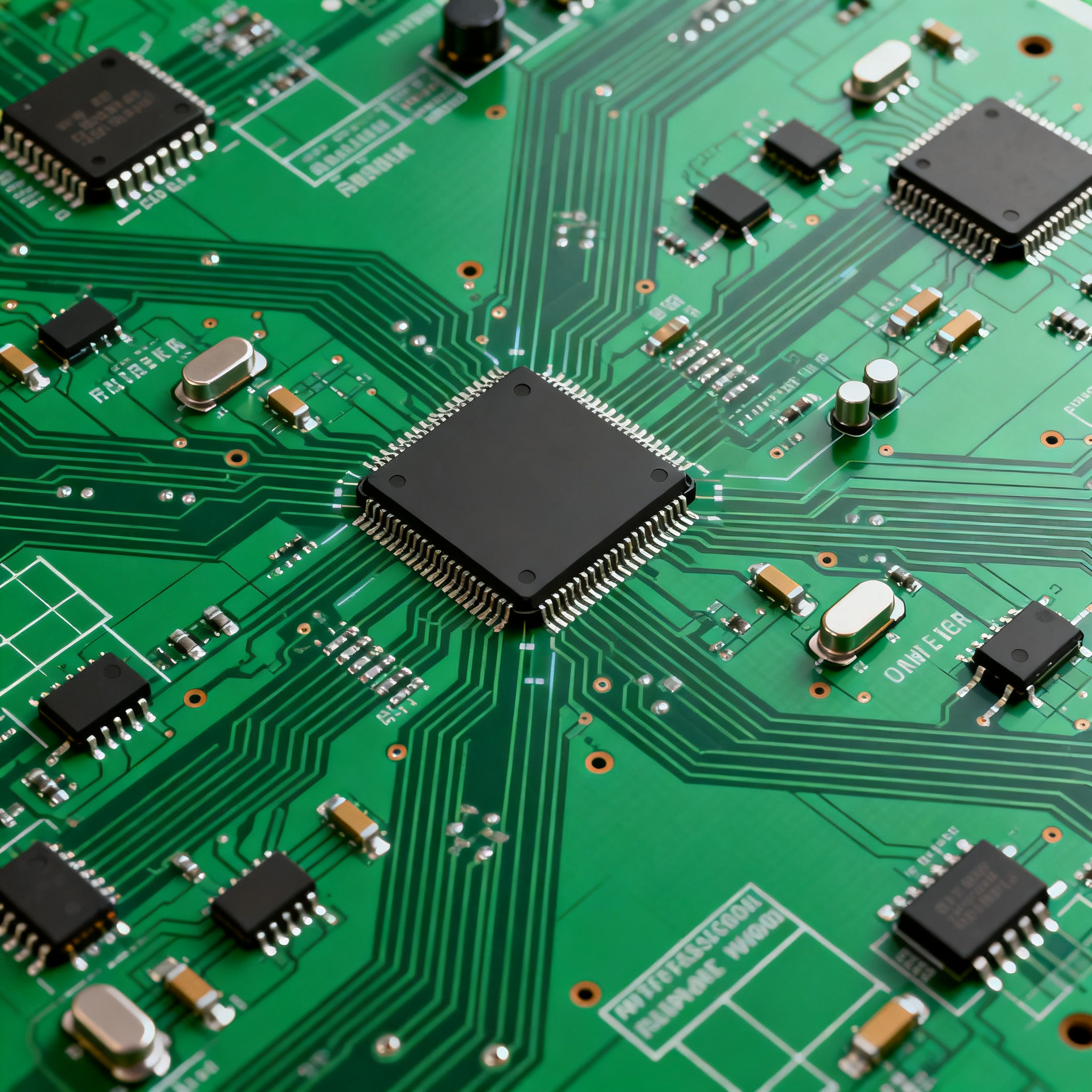
Electromagnetic interference (EMI) refers to the unwanted disturbance caused by electromagnetic fields affecting the performance of electronic circuits. In PCB design, EMI can originate from various sources, including power supplies, signal traces, and external devices. To address EMI concerns, engineers must focus on the core principles of design architecture, such as grounding, shielding, and filtering. The architecture of a PCB layout plays a critical role in mitigating EMI. Ground planes, for instance, provide low-resistance paths that help reduce noise. Meanwhile, shielding techniques protect sensitive components from external interference. Filtering components, like capacitors and inductors, are used to suppress high-frequency noise. By integrating these principles, designers can create PCBs that not only meet performance standards but also comply with regulatory requirements.
Detailed Specifications
When designing PCBs for EMI compliance, understanding component specifications is vital. Key parameters such as impedance, capacitance, and inductance directly impact a circuit's susceptibility to EMI. Additionally, thermal characteristics and material properties influence the overall performance and reliability of the PCB. Selecting components with the right specifications ensures that the design meets both functional and regulatory standards. Below is a table summarizing the key specifications crucial for EMI-compliant PCB design.
| Parameter | Specification | Importance |
|---|---|---|
| Impedance | 50 Ohms | Ensures signal integrity and minimizes reflections |
| Capacitance | 10 pF | Reduces high-frequency noise |
| Inductance | 1 nH | Prevents unwanted coupling |
| Resonant Frequency | 2 GHz | Avoids interference at operational frequencies |
| Dielectric Constant | 4.5 | Affects signal speed and impedance |
| Thermal Conductivity | 0.8 W/mK | Ensures heat dissipation |
| Loss Tangent | 0.02 | Impacts signal attenuation |
| Max Voltage Rating | 100V | Prevents breakdown under high voltage |
| Operating Temperature | -40°C to 85°C | Ensures performance in varied conditions |
| Material Type | FR-4 | Commonly used PCB substrate |
| Copper Thickness | 1 oz/ft² | Influences current carrying capacity |
Key Takeaways from the Specifications
The specifications outlined in the table above are critical for designing PCBs that are EMI compliant. Impedance matching is essential to maintain signal integrity and reduce reflections, while capacitance and inductance values play pivotal roles in filtering high-frequency noise and preventing electromagnetic coupling. The resonant frequency should be chosen to avoid interference within the operational frequency range. Thermal and dielectric properties, such as thermal conductivity and dielectric constant, influence both the electrical and thermal performance of the PCB. Selecting materials like FR-4 with appropriate copper thickness ensures the board can handle the required current loads without overheating.
| Metric | Value | Significance |
|---|---|---|
| Signal Attenuation | 0.5 dB/cm | Affects signal strength over distance |
| Thermal Resistance | 30°C/W | Impacts heat dissipation efficiency |
| Power Dissipation | 1 W | Limits power handling capability |
| Current Capacity | 2A | Determines maximum current flow |
| Voltage Standing Wave Ratio (VSWR) | 1.2:1 | Indicates impedance matching quality |
| Noise Figure | 3 dB | Measures signal-to-noise ratio degradation |
| Electromagnetic Compatibility (EMC) | Compliant | Ensures minimal interference with other devices |
| Thermal Expansion Coefficient | 17 ppm/°C | Ensures mechanical stability |
| Surface Finish | HASL | Provides good solderability |
Practical Implications
The performance metrics in this table highlight the electrical and thermal characteristics crucial for EMI compliance. Signal attenuation and VSWR are important for maintaining signal strength and ensuring impedance matching, respectively. A low noise figure is desirable to maintain a high signal-to-noise ratio. Thermal metrics like thermal resistance and expansion coefficient ensure that the PCB can dissipate heat effectively and maintain mechanical stability under varying temperatures. The power dissipation rating and current capacity are critical for determining the power handling capability of the PCB, while the surface finish impacts solderability and overall reliability.
| Use Case | Configuration | Benefits |
|---|---|---|
| Consumer Electronics | Single Layer | Cost-effective, simple designs |
| Automotive Systems | Multi-layer | Enhanced reliability, reduced EMI |
| Telecommunications | High-Frequency | Supports high-speed data transfer |
| Medical Devices | Flex PCB | Compact, adaptable to various shapes |
| Industrial Equipment | Rigid-Flex | Durability, flexibility in harsh environments |
| Aerospace Applications | High-Temperature | Performance under extreme conditions |
| IoT Devices | Miniaturized | Space-saving, efficient designs |
Application Guidelines
The application matrix outlines various use cases and configurations that benefit from specific PCB designs. Consumer electronics often utilize single-layer boards for cost efficiency, while automotive systems leverage multi-layer designs to enhance reliability and reduce EMI. Telecommunications require high-frequency configurations to support fast data transfer rates. Medical devices benefit from flexible PCBs due to their compactness and adaptability. Rigid-flex designs offer industrial equipment durability and flexibility in harsh environments. Aerospace applications demand high-temperature PCBs for performance under extreme conditions, and IoT devices thrive on miniaturized designs to save space and improve efficiency.
Design Considerations
Designing PCBs for EMI compliance involves a multitude of considerations. Firstly, understanding the operational environment is crucial. Factors such as temperature, humidity, and potential exposure to electromagnetic fields must be considered. Utilizing ground planes effectively can significantly reduce EMI by providing a low-inductance path for return currents. Shielding sensitive components and using proper trace routing techniques can further mitigate interference. The selection of materials also plays a vital role; using high-quality substrates and surface finishes can enhance both electrical performance and durability. Additionally, the placement of components affects EMI susceptibility. Critical components should be strategically placed to minimize loop areas and avoid signal crosstalk. Implementing filter components such as ferrite beads and decoupling capacitors can help suppress high-frequency noise. Finally, adherence to industry standards, such as those set by IPC, ensures that designs meet both performance and regulatory requirements, providing a roadmap for successful PCB design.
Step-by-Step Implementation
Creating a PCB layout that is compliant with EMI standards involves a structured approach. Here is a step-by-step guide:
- Define Requirements: Start by understanding the functional and regulatory requirements of your design. This includes identifying the operating frequency, power levels, and environmental conditions.
- Schematic Design: Develop a detailed schematic that outlines the electrical connections between components. Pay attention to signal integrity and ensure that decoupling capacitors are included to filter noise.
- Component Placement: Strategically place components to minimize loop areas and reduce the potential for crosstalk. Keep sensitive components away from noisy sections of the board.
- Routing: Route traces with impedance control in mind. Use short and direct paths for high-frequency signals and ensure adequate spacing between traces to prevent coupling.
- Grounding: Implement solid ground planes to provide a low-inductance return path for signals. This helps in reducing EMI emissions and improves overall signal integrity.
- Shielding and Filtering: Use shielding techniques for sensitive components and incorporate filtering components like ferrite beads and capacitors to suppress unwanted noise.
- Thermal Management: Ensure proper thermal management by placing thermal vias and heat sinks where necessary to dissipate heat effectively.
- Design Review and Simulation: Conduct a thorough design review and use simulation tools to predict EMI performance. Make necessary adjustments based on simulation results.
Common Issues & Solutions
Even with careful planning, several common issues can arise in PCB design for EMI compliance. Here are some problems and their solutions:
- Signal Crosstalk: To prevent crosstalk, ensure adequate spacing between traces and use ground planes to provide isolation.
- Ground Loop Issues: Avoid ground loops by designing a single-point grounding system and using a star-grounding technique.
- Thermal Overload: Address thermal issues by incorporating thermal vias, heat sinks, and ensuring sufficient airflow over the PCB.
- Impedance Mismatch: Use impedance-controlled traces and matching networks to minimize reflections and improve signal integrity.
- Component Placement Conflicts: Resolve placement conflicts by revisiting the layout and ensuring critical components are prioritized in the design.
- Regulatory Non-Compliance: Stay updated with the latest regulations and standards, and conduct pre-compliance testing to identify potential issues early.
Applications & Use Cases
PCBs designed for EMI compliance find applications across various industries. In consumer electronics, they ensure devices operate without interference from nearby gadgets. Automotive systems benefit from EMI-compliant PCBs by maintaining reliable communication and control in vehicles. In telecommunications, these PCBs support high-speed data transmission with minimal signal loss. Medical devices rely on EMI compliance for accurate and reliable operation in critical health monitoring equipment. Industrial equipment often operates in harsh environments, where EMI-compliant PCBs ensure robust performance. Lastly, in aerospace applications, maintaining EMI compliance is essential for the safety and reliability of avionics systems.
Selection & Sourcing Guide
Selecting the right components for EMI-compliant PCBs is crucial. Engineers should refer to datasheets and component specifications to ensure compatibility with design requirements. For sourcing, IC Online offers a comprehensive platform to find and compare components from various manufacturers. Consider factors such as lead time, cost, and availability when making purchasing decisions. Collaborating with reliable suppliers ensures access to quality components that meet both performance and regulatory standards.
FAQ
- What is EMI in PCB design? EMI, or electromagnetic interference, is the disruption caused by electromagnetic fields affecting electronic circuits.
- Why is EMI compliance important? EMI compliance ensures that electronic devices operate reliably and do not interfere with other devices, meeting regulatory standards.
- How can I minimize EMI in my PCB design? Use techniques such as grounding, shielding, and filtering to reduce EMI. Proper component placement and routing also play a critical role.
- What are the key specifications to consider for EMI compliance? Important specifications include impedance, capacitance, inductance, thermal conductivity, and dielectric constant.
- How does component placement affect EMI? Strategic component placement minimizes loop areas and reduces the potential for signal crosstalk, improving EMI performance.
- What role do ground planes play in EMI reduction? Ground planes provide a low-inductance path for return currents, reducing noise and improving signal integrity.
- Are there specific materials recommended for EMI-compliant PCBs? Materials like FR-4 are commonly used, but the choice depends on the specific requirements of the application, such as thermal performance and dielectric properties.
- How do I ensure my design meets regulatory standards? Adhering to industry standards, conducting pre-compliance testing, and staying updated with regulations are essential for meeting EMI compliance.
- What tools can help in designing EMI-compliant PCBs? Simulation tools and design software with EMI analysis capabilities can help predict and mitigate potential EMI issues.
- Can EMI compliance affect the cost of PCB design? While EMI compliance may increase design complexity and cost, it ensures reliability and regulatory adherence, potentially reducing long-term costs associated with non-compliance.
Conclusion
Designing PCB layouts for EMI compliance is a critical aspect of modern electronics engineering. By understanding and applying key specifications, performance metrics, and application guidelines, engineers can create designs that meet both functional and regulatory requirements. Implementing effective design strategies and staying informed about industry standards ensures that electronic devices operate reliably and efficiently in diverse environments. Ultimately, achieving EMI compliance not only enhances the performance and reliability of electronic systems but also fosters innovation by enabling the development of advanced technologies.