Designing PCB Layouts for EMI Compliance: Essential Techniques for 4-Layer Boards
Designing PCB Layouts for EMI Compliance: Essential Techniques for 4-Layer Boards Introduction In the world of electronics, designing a PCB (Printed Circuit Board) layout that complies with Electromag...
Introduction
In the world of electronics, designing a PCB (Printed Circuit Board) layout that complies with Electromagnetic Interference (EMI) standards is crucial for ensuring the reliability and performance of electronic devices. As electronic devices become more complex, the demand for efficient and EMI-compliant PCB designs increases. A 4-layer board offers a balanced approach between complexity and cost, making it a popular choice for many applications. This article delves into the essential techniques for designing EMI-compliant PCB layouts, focusing on circuit topology, component calculations, performance analysis, and design trade-offs.
Technical Overview
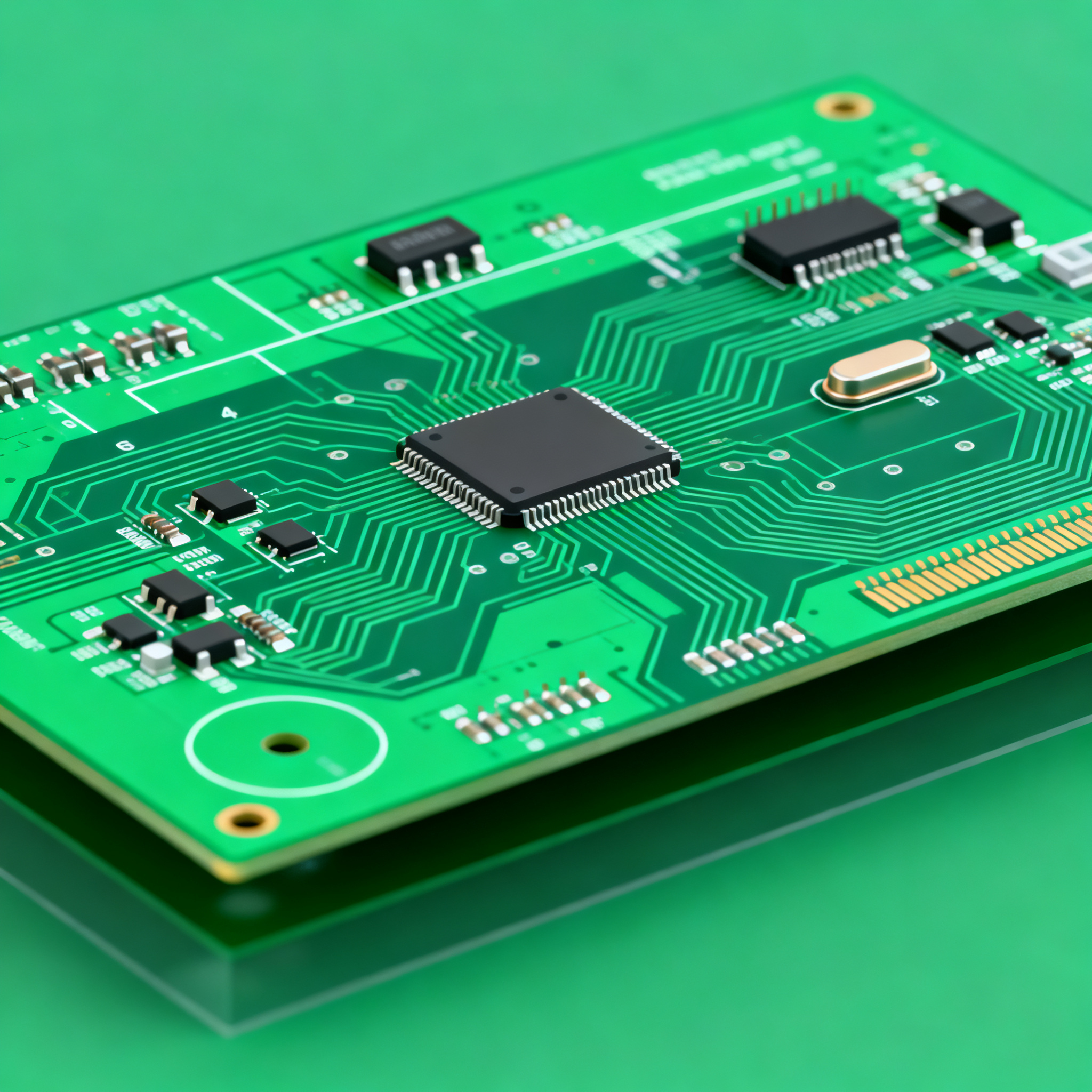
The core concept of EMI compliance in PCB design revolves around minimizing electromagnetic emissions and susceptibility. This involves careful consideration of trace routing, component placement, and layer stack-up. A typical 4-layer board consists of a top layer for components and traces, an internal layer for power or ground, another internal layer for signal routing, and a bottom layer for additional components or grounding. The architecture of a 4-layer board allows for effective signal integrity management and EMI control by providing dedicated ground and power planes. Key principles include minimizing loop areas, using differential signaling, and employing proper grounding techniques.
Understanding the principles of EMI compliance requires familiarity with IPC standards, such as IPC-A-610 and IPC-2221, which provide guidelines for PCB design and manufacturing. These standards ensure that the board meets quality and performance criteria. Additionally, resources from manufacturers like PCBWay and Nova PCBA offer insights into the manufacturing capabilities and design rules that can impact EMI performance. By integrating these principles and resources, designers can create PCB layouts that effectively reduce EMI and enhance device performance.
Detailed Specifications
When designing a PCB for EMI compliance, several specifications are critical. These include component values, trace widths, layer stack-up, and grounding strategies. Calculations for impedance matching, signal integrity, and power distribution must be precise to ensure optimum performance. The table below outlines key design parameters that influence EMI compliance in a 4-layer PCB.
| Component/Parameter | Value/Formula | Description |
|---|---|---|
| Trace Width | 0.2 mm | Width of the signal traces to maintain impedance |
| Impedance | 50 Ω | Characteristic impedance for signal integrity |
| Layer Stack-up | Signal-Ground-Power-Signal | Common 4-layer configuration for EMI reduction |
| Ground Plane | Continuous | Ensures low impedance return path |
| Via Diameter | 0.3 mm | Size of vias for inter-layer connections |
| Capacitor Value | 10 nF | Decoupling capacitor for power supply noise reduction |
| Inductor Value | 100 µH | Used for filtering and EMI suppression |
| Signal Rise Time | 1 ns | Time for signal to transition, affects EMI |
| Trace Separation | 0.5 mm | Distance between traces to prevent crosstalk |
| Power Plane | Isolated | Separate power plane to prevent noise coupling |
| Shielding | Conductive Enclosure | Physical barrier to prevent EMI |
Key Takeaways from the Specifications
The design parameters outlined in the table highlight the critical aspects of achieving EMI compliance in a 4-layer PCB design. Trace width and impedance are vital for maintaining signal integrity, while a well-defined layer stack-up helps in reducing electromagnetic emissions. The use of continuous ground planes and isolated power planes ensures low impedance return paths and minimizes noise coupling. Decoupling capacitors and inductors are essential for filtering and suppressing noise, thereby improving the board's overall performance. By adhering to these specifications, designers can effectively manage EMI and enhance the reliability of their electronic devices.
| Performance Metric | Value | Impact |
|---|---|---|
| Gain | 10 dB | Amplification of signal, affects output strength |
| Bandwidth | 2 GHz | Range of frequencies the PCB can handle |
| Noise Figure | 3 dB | Measure of noise contribution, lower is better |
| Power Consumption | 5 W | Amount of power used by the PCB |
| Signal-to-Noise Ratio | 60 dB | Quality of the signal compared to background noise |
| Return Loss | -15 dB | Reflection of signal, lower means better match |
| Harmonic Distortion | 0.5% | Unwanted harmonics in signal, lower preferred |
| Temperature Range | -40°C to 85°C | Operational temperature limits of the PCB |
| Latency | 10 ns | Delay in signal processing, affects real-time applications |
| Efficiency | 85% | Ratio of useful power output to total power input |
Practical Implications
The performance metrics provided in the table offer insights into the operational capabilities of a 4-layer PCB. Gain and bandwidth are crucial for determining the board's ability to handle high-frequency signals, while the noise figure and signal-to-noise ratio indicate the quality of signal transmission. Power consumption and efficiency are important for assessing the energy requirements and sustainability of the design. Understanding these metrics allows designers to optimize their PCB layouts for specific applications, ensuring that the boards meet the necessary performance criteria while maintaining EMI compliance.
| Configuration | Pros | Cons |
|---|---|---|
| Single-Ended Routing | Simple Design | Higher EMI |
| Differential Pair Routing | Reduced EMI | More Complex Design |
| Star Grounding | Minimizes Ground Loops | Complex Implementation |
| Plane Grounding | Simple to Implement | Potential for Ground Loops |
| Shielded Traces | Excellent EMI Reduction | Higher Cost |
| Unshielded Traces | Cost-Effective | Higher EMI |
| Wide Traces | Lower Resistance | More Space Required |
| Narrow Traces | Saves Space | Higher Resistance |
Application Guidelines
The design trade-offs illustrated in the table highlight the various configurations available for 4-layer PCB layouts and their respective advantages and disadvantages. Differential pair routing is favored for its EMI reduction capabilities, despite its complexity. Star grounding offers excellent ground loop minimization but can be challenging to implement. Shielded traces provide superior EMI protection but at a higher cost. Selecting the appropriate configuration depends on the specific application requirements, budget constraints, and desired performance outcomes. By carefully evaluating these trade-offs, designers can make informed decisions to optimize their PCB designs for EMI compliance.
Design Considerations
Designing a 4-layer PCB layout for EMI compliance involves several practical considerations to ensure optimal performance. One of the key aspects is the careful placement of components. Critical components should be placed close to their corresponding connectors to minimize trace lengths and reduce the potential for EMI. Additionally, the use of decoupling capacitors near power pins can help suppress high-frequency noise and stabilize the power supply.
Another important consideration is the routing of signal traces. Keeping traces short and direct helps minimize inductance and reduce the potential for crosstalk. When routing differential pairs, maintaining equal trace lengths and consistent spacing is crucial for preserving signal integrity. Implementing a ground fill on the signal layers can further enhance EMI performance by providing a low-impedance return path.
The layer stack-up of a 4-layer PCB also plays a significant role in EMI compliance. A commonly used configuration is Signal-Ground-Power-Signal, which provides effective isolation between power and signal layers. This stack-up allows for efficient power distribution and reduces electromagnetic emissions. When designing the stack-up, it's essential to ensure that the ground and power planes are continuous and free of splits to prevent EMI issues.
Finally, the selection of materials and fabrication processes can impact the EMI performance of the PCB. High-quality materials with low dielectric losses and controlled impedance can enhance signal integrity. Collaborating with experienced PCB manufacturers, such as PCBWay and Nova PCBA, can provide valuable insights into material selection and fabrication techniques that align with EMI compliance goals.
Step-by-Step Implementation
- Define Design Requirements: Start by identifying the specific requirements for your PCB design, including performance, size, and EMI compliance. Refer to industry standards such as IPC-A-610 and IPC-2221 for guidance.
- Create a Schematic: Develop a detailed schematic diagram that outlines the circuit topology and component connections. Ensure that the schematic aligns with the design requirements and EMI compliance goals.
- Design the Layer Stack-up: Choose an appropriate layer stack-up for your 4-layer PCB. A common configuration is Signal-Ground-Power-Signal, which offers effective EMI control and signal integrity.
- Place Components: Strategically place components on the PCB, prioritizing critical components near connectors. Use decoupling capacitors near power pins to reduce high-frequency noise.
- Route Signal Traces: Route signal traces with minimal length and direct paths to reduce inductance. Use differential pair routing for high-speed signals, maintaining equal trace lengths and consistent spacing.
- Implement Ground and Power Planes: Ensure continuous ground and power planes with no splits. Use ground fills on signal layers to provide low-impedance return paths and enhance EMI performance.
- Perform Design Rule Checks: Conduct thorough design rule checks to ensure that the PCB layout adheres to manufacturing guidelines and EMI compliance standards.
- Prototype and Test: Fabricate a prototype of the PCB and conduct testing to verify its performance. Measure key parameters such as gain, bandwidth, noise figure, and EMI emissions to ensure compliance.
Common Issues & Solutions
- Issue: Crosstalk Between Traces
Solution: Increase the separation between signal traces and use ground fills to minimize crosstalk. - Issue: EMI from Power Supply
Solution: Use decoupling capacitors near power pins and implement an isolated power plane to reduce EMI. - Issue: Ground Loop Interference
Solution: Employ a star grounding configuration to minimize ground loops and improve EMI performance. - Issue: Signal Reflection
Solution: Ensure proper impedance matching by adjusting trace widths and using termination resistors. - Issue: Excessive Heat Generation
Solution: Optimize the thermal management by using wider traces and thermal vias to dissipate heat effectively. - Issue: Inadequate Signal Integrity
Solution: Use differential pair routing for high-speed signals and maintain consistent trace lengths and spacing.
Applications & Use Cases
EMI-compliant 4-layer PCB designs are widely used in various applications, including telecommunications, automotive electronics, and consumer electronics. In telecommunications, these designs are essential for ensuring reliable signal transmission and reducing interference in RF circuits. Automotive electronics benefit from EMI-compliant PCBs by enhancing the performance and safety of electronic control units (ECUs) and infotainment systems. In consumer electronics, such as smartphones and tablets, EMI compliance is crucial for maintaining signal integrity and reducing electromagnetic emissions that could affect device performance and user experience.
Selection & Sourcing Guide
Selecting the right components and materials for EMI-compliant PCB designs is critical for achieving optimal performance. Consider collaborating with reputable suppliers and manufacturers who specialize in EMI-compliant materials and components. For sourcing integrated circuits and other electronic components, visit IC Online, a reliable platform for procuring high-quality electronic components.
FAQ
- What is EMI compliance in PCB design?
EMI compliance involves designing PCBs to minimize electromagnetic interference emissions and susceptibility, ensuring reliable device performance. - Why is a 4-layer board preferred for EMI compliance?
A 4-layer board offers a balanced approach between complexity and cost, providing dedicated ground and power planes for effective EMI control. - How does differential pair routing reduce EMI?
Differential pair routing reduces EMI by using two complementary signals that cancel out electromagnetic emissions and enhance signal integrity. - What role do decoupling capacitors play in EMI compliance?
Decoupling capacitors suppress high-frequency noise and stabilize the power supply, reducing EMI and improving overall PCB performance. - How can I ensure proper impedance matching in my PCB design?
Proper impedance matching can be achieved by adjusting trace widths, using termination resistors, and adhering to impedance control guidelines. - What are the benefits of using continuous ground planes?
Continuous ground planes provide low impedance return paths, minimize ground loops, and enhance EMI performance. - How do I select the right materials for EMI-compliant PCBs?
Choose materials with low dielectric losses and controlled impedance, and consult with experienced manufacturers for guidance on material selection. - Can EMI compliance affect the cost of PCB design?
While EMI compliance may involve additional design considerations and materials, the long-term benefits of improved performance and reliability often outweigh the costs. - What testing methods are used to verify EMI compliance?
Testing methods include measuring key performance metrics such as gain, bandwidth, noise figure, and electromagnetic emissions to ensure compliance. - How can I collaborate with manufacturers for EMI-compliant designs?
Work with reputable manufacturers like PCBWay and Nova PCBA, who offer insights into design rules, material selection, and fabrication techniques for EMI compliance.
Conclusion
Designing EMI-compliant PCB layouts for 4-layer boards requires a comprehensive understanding of circuit topology, component calculations, and performance analysis. By adhering to key design parameters, optimizing layer stack-up, and carefully evaluating design trade-offs, engineers can create PCB layouts that minimize electromagnetic interference and enhance device performance. Collaborating with experienced manufacturers and sourcing high-quality components are crucial steps towards achieving EMI compliance. Ultimately, these efforts contribute to the development of reliable and efficient electronic devices that meet industry standards and user expectations.