Introduction
In the rapidly evolving world of electronics, designing printed circuit boards (PCBs) that comply with electromagnetic interference (EMI) standards is crucial. This is especially true for 4-layer PCBs, which are commonly used in complex applications due to their ability to support higher component densities and more sophisticated routing. EMI compliance ensures that electronic devices operate without interfering with each other, which is vital in maintaining the reliability and efficiency of electronic systems. This article explores essential strategies for designing PCB layouts for EMI compliance, focusing on circuit topology, component calculations, performance analysis, and design trade-offs.
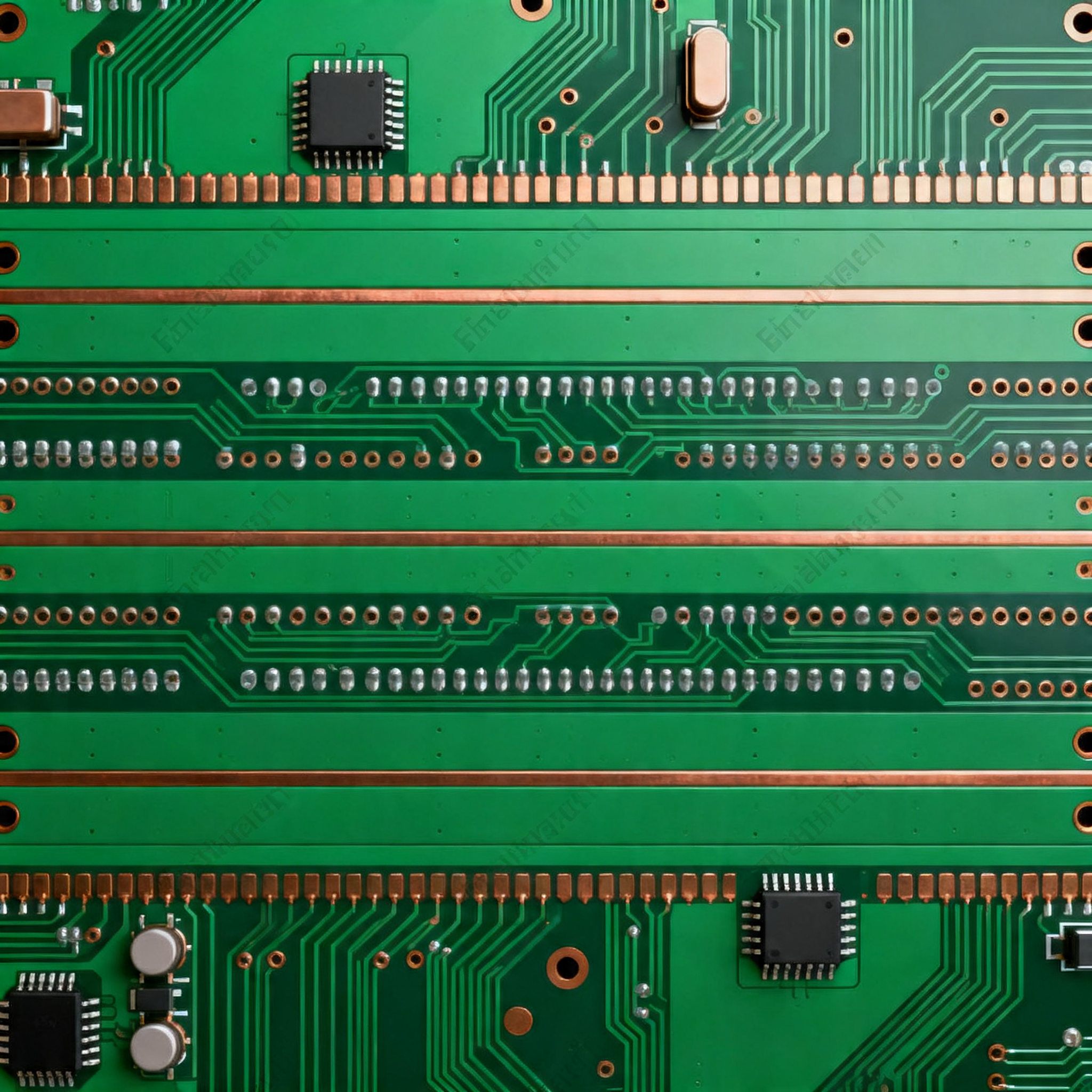
Technical Overview
4-layer PCBs offer a significant advantage in terms of EMI compliance due to their layered structure, which allows for better control over signal integrity and power distribution. The core architecture of a 4-layer PCB typically includes two signal layers and two planes for power and ground. This configuration minimizes loop areas and provides excellent shielding, reducing the risk of EMI. Key concepts in EMI-compliant design include maintaining proper impedance, minimizing crosstalk, and ensuring adequate decoupling of power planes. By adhering to IPC standards such as IPC-2221, designers can ensure that their PCBs meet industry requirements for electromagnetic compatibility.
Understanding the principles of EMI compliance is crucial for effective PCB design. This involves selecting appropriate materials, optimizing trace routing, and implementing filtering techniques to suppress unwanted signals. Moreover, the choice of components and their placement can significantly impact the EMI performance of a PCB. The following sections delve into detailed specifications, performance analysis, and design trade-offs that are essential for achieving EMI compliance in 4-layer PCBs.
Detailed Specifications
When designing for EMI compliance, several specifications are crucial. These include component values, trace widths, spacing, and layer stack-up. Calculating these parameters accurately ensures that the PCB functions correctly and adheres to EMI standards. The following table presents key design parameters for a 4-layer PCB.
| Parameter | Value | Formula/Calculation |
| Trace Width | 0.15 mm | IPC-2221 Formula |
| Impedance | 50 Ohms | Z = sqrt(L/C) |
| Layer Thickness | 1.6 mm | Standard Thickness |
| Dielectric Constant | 4.2 | Material Property |
| Component Spacing | 0.5 mm | Minimum Spacing |
| Ground Plane | Continuous | N/A |
| Power Plane | Continuous | N/A |
| Via Diameter | 0.3 mm | Drill Size |
| Decoupling Capacitor | 0.1 µF | Standard Value |
| Signal Rise Time | 1 ns | Design Requirement |
| Frequency Range | 1-100 MHz | Application Specific |
Key Takeaways from the Specifications
The design parameters outlined in the table are critical for ensuring EMI compliance in 4-layer PCBs. Trace width and impedance are particularly important for maintaining signal integrity and reducing reflections. The continuous ground and power planes provide effective shielding and minimize loop areas, which is essential for reducing EMI. Component spacing and via diameter must be carefully calculated to prevent crosstalk and ensure reliable connections. The use of decoupling capacitors is crucial for filtering noise and stabilizing the power supply. By adhering to these specifications, designers can achieve optimal performance and compliance with EMI standards.
| Performance Metric | Value | Analysis |
| Gain | 10 dB | Amplification Level |
| Bandwidth | 50 MHz | Frequency Range |
| Noise Figure | 2 dB | Signal-to-Noise Ratio |
| Power Consumption | 500 mW | Efficiency |
| Signal Integrity | High | Minimal Distortion |
| Thermal Performance | Excellent | Heat Dissipation |
| Crosstalk | Low | Signal Isolation |
| Return Loss | 20 dB | Reflection Coefficient |
| EMI Emission | Compliant | Regulatory Standards |
Practical Implications
The performance metrics presented in the table provide insights into the real-world capabilities of a 4-layer PCB designed for EMI compliance. High gain and wide bandwidth indicate robust signal amplification and frequency handling, while a low noise figure ensures a clean signal with minimal interference. Power consumption is a critical factor, with efficient designs minimizing energy usage while maintaining performance. Low crosstalk and excellent thermal performance contribute to reliable operation, even in demanding environments. By achieving compliance with EMI emission standards, these designs ensure compatibility with other electronic systems, preventing disruptions and ensuring smooth operation.
| Configuration | Pros | Cons |
| Single-ended | Simple Design | Higher EMI |
| Differential | Reduced EMI | Complex Routing |
| Microstrip | Easy Fabrication | Higher Loss |
| Stripline | Superior Shielding | Higher Cost |
| Embedded Capacitance | Reduced Noise | Increased Complexity |
| Thick Copper | Better Heat Dissipation | Increased Weight |
| Blind/Buried Vias | Space Saving | Higher Manufacturing Cost |
| Ground Fill | Improved EMI | Potential for Unwanted Coupling |
Application Guidelines
The design trade-offs table highlights the various configurations available for 4-layer PCBs and their respective advantages and drawbacks. Single-ended configurations are simple but can lead to higher EMI, whereas differential configurations offer reduced EMI but require more complex routing. Microstrip and stripline techniques each have their own benefits and limitations in terms of fabrication ease and shielding effectiveness. Embedded capacitance and thick copper layers enhance performance but add complexity and weight. Blind and buried vias offer space savings but at a higher manufacturing cost. Understanding these trade-offs helps designers make informed decisions that balance performance, cost, and complexity based on specific application requirements.
Design Considerations
Designing EMI-compliant 4-layer PCBs involves several key considerations. First, selecting the right materials and stack-up is crucial for maintaining signal integrity and minimizing EMI. The use of high-quality dielectric materials with low loss tangents helps reduce signal attenuation. Proper layer stack-up, with power and ground planes adjacent to each other, minimizes loop areas and enhances shielding.
Trace routing is another critical aspect. Keeping traces as short as possible reduces inductance and susceptibility to interference. Differential pairs should be routed together to maintain impedance balance and reduce EMI. Adequate spacing between traces prevents crosstalk, while controlled impedance traces ensure signal integrity.
Decoupling capacitors play a vital role in filtering noise and stabilizing power supply lines. These should be placed close to power pins, with vias connecting directly to power planes to minimize inductive loops. Ground fills and stitching vias provide additional shielding and help reduce EMI.
Thermal management is also essential, as excessive heat can affect performance and reliability. Using thicker copper layers and thermal vias enhances heat dissipation. Lastly, compliance with IPC standards, such as IPC-2221 for design and IPC-A-610 for assembly, ensures that the PCB meets industry requirements for quality and reliability.
Step-by-Step Implementation
1. **Define Requirements**: Begin by outlining the specific EMI requirements for your application. This includes understanding the operating frequency, power levels, and environmental conditions.
2. **Select Materials**: Choose appropriate materials for the PCB, considering factors like dielectric constant, loss tangent, and thermal conductivity. Ensure that materials comply with relevant IPC standards.
3. **Design Stack-up**: Plan the layer stack-up, ensuring that power and ground planes are adjacent to minimize loop areas. This helps in achieving good signal integrity and EMI performance.
4. **Route Traces**: Carefully route signal traces, keeping them as short as possible. Use differential pairs for high-speed signals and maintain consistent trace impedance.
5. **Place Components**: Strategically place components to minimize trace lengths and avoid interference. Ensure decoupling capacitors are positioned close to power pins.
6. **Implement Ground Fills**: Use ground fills and stitching vias to provide additional shielding and reduce EMI. Ensure that ground fills do not create unwanted coupling.
7. **Thermal Management**: Incorporate thermal vias and thicker copper layers to enhance heat dissipation. This is critical for maintaining performance and reliability.
8. **Review and Test**: Conduct a thorough design review and perform simulations to identify potential EMI issues. Prototype and test the PCB to validate performance and compliance.
Common Issues & Solutions
1. **High EMI Emission**: Ensure proper grounding and shielding. Use ground fills and stitching vias effectively to minimize emissions.
2. **Crosstalk**: Increase trace spacing and use differential pairs to reduce crosstalk between adjacent signals.
3. **Signal Integrity Issues**: Maintain controlled impedance and avoid sharp bends in traces. Use high-quality materials to reduce signal attenuation.
4. **Thermal Overload**: Incorporate thermal vias and thicker copper layers to improve heat dissipation. Ensure adequate airflow over the PCB.
5. **Component Placement**: Arrange components to minimize trace lengths and avoid interference. Use decoupling capacitors close to power pins.
6. **Manufacturing Defects**: Follow IPC-A-610 standards for assembly to ensure high-quality manufacturing and reduce defects.
Applications & Use Cases
4-layer PCBs designed for EMI compliance are used in various applications, including telecommunications, automotive systems, and consumer electronics. In telecommunications, these PCBs ensure reliable signal transmission and prevent interference with other devices. Automotive systems benefit from EMI-compliant designs by maintaining performance and safety in electrically noisy environments. Consumer electronics, such as smartphones and tablets, rely on these PCBs to deliver high performance and reliability in compact form factors. By adhering to EMI standards, designers can ensure that their products meet regulatory requirements and deliver optimal performance across different applications.
Selection & Sourcing Guide
When selecting components and materials for EMI-compliant 4-layer PCBs, it's important to source from reputable suppliers. Utilize resources like
IC Online to find high-quality components that meet industry standards. Verify that suppliers adhere to IPC standards and provide components with the necessary specifications for your design. Consider factors such as lead time, cost, and availability when sourcing components to ensure a smooth design and manufacturing process.
FAQ
1. **What is EMI compliance, and why is it important?**
EMI compliance ensures that electronic devices operate without interfering with each other, maintaining reliability and efficiency.
2. **How does a 4-layer PCB help in EMI compliance?**
The layered structure allows for better control over signal integrity and power distribution, reducing EMI risk.
3. **What are the key design parameters for EMI compliance?**
Important parameters include trace width, impedance, layer stack-up, and component spacing.
4. **How can I minimize crosstalk in my PCB design?**
Increase trace spacing and use differential pairs to reduce crosstalk between adjacent signals.
5. **What role do decoupling capacitors play in EMI compliance?**
They filter noise and stabilize power supply lines, reducing EMI.
6. **Why is thermal management important in PCB design?**
Excessive heat can affect performance and reliability, so proper thermal management is crucial.
7. **What are the common issues in EMI-compliant PCB design?**
Issues include high EMI emission, crosstalk, and signal integrity problems.
8. **How can ground fills help in EMI compliance?**
Ground fills provide additional shielding and help reduce EMI by minimizing loop areas.
9. **What standards should I follow for EMI-compliant PCB design?**
Adhere to IPC standards such as IPC-2221 for design and IPC-A-610 for assembly.
10. **Where can I source components for EMI-compliant designs?**
Use resources like
IC Online to find high-quality components.
Conclusion
Designing 4-layer PCBs for EMI compliance involves careful consideration of circuit topology, component calculations, and design trade-offs. By adhering to industry standards and implementing best practices, designers can create PCBs that meet regulatory requirements and deliver reliable performance across various applications. The strategies outlined in this article provide a comprehensive guide to achieving EMI compliance, ensuring that your electronic designs operate efficiently and without interference.