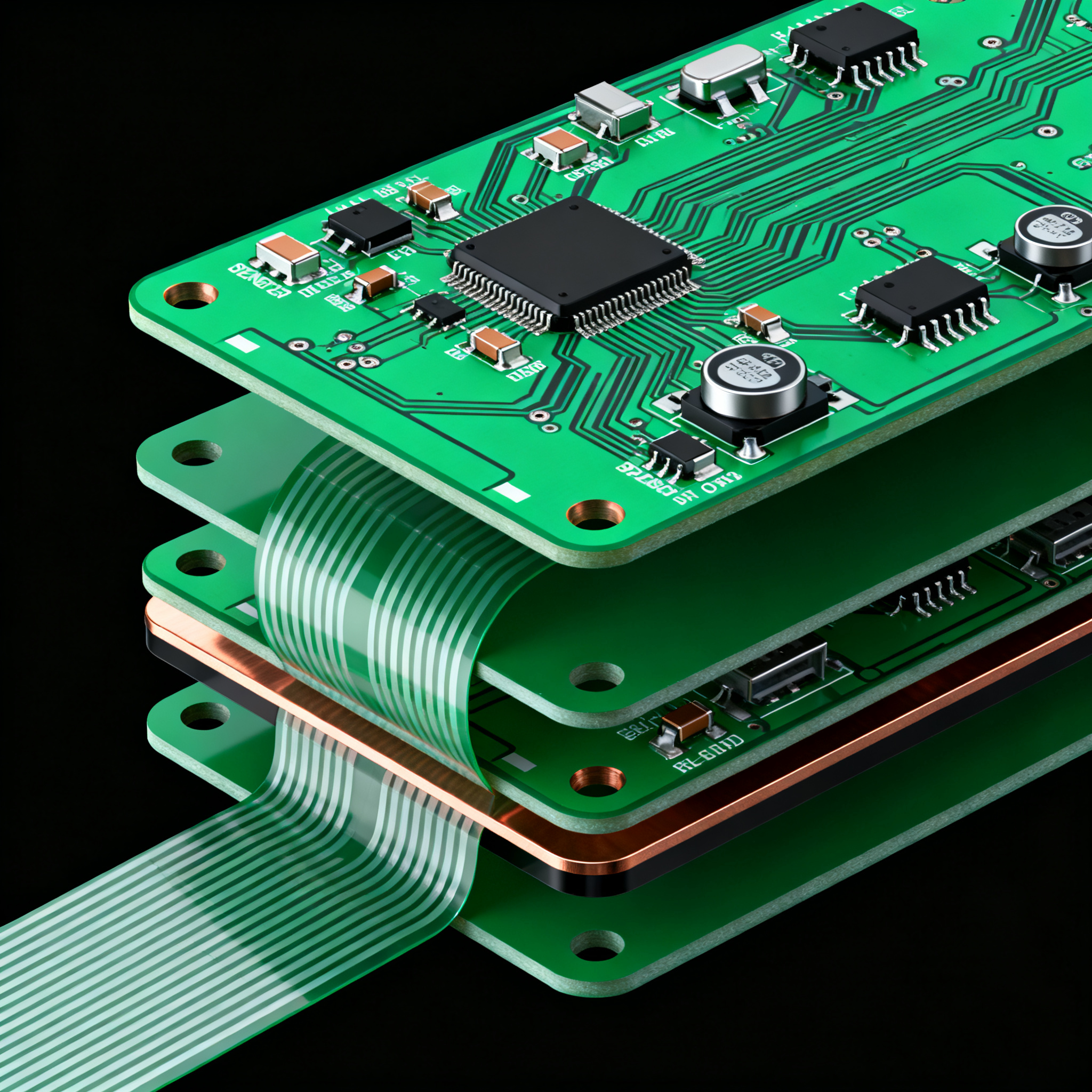
Designing a 4-Layer Rigid-Flex PCB for IoT Sensor Nodes: A Step-by-Step Manufacturing and Assembly Guide
Designing a 4-Layer Rigid-Flex PCB for IoT Sensor Nodes: A Step-by-Step Guide from Stack-Up to Flying Probe Test Why IoT Sensor Nodes Are Outgrowing 2-Layer Boards—and How Rigid-Flex Delivers a Compac...
Designing a 4-Layer Rigid-Flex PCB for IoT Sensor Nodes: A Step-by-Step Guide from Stack-Up to Flying Probe Test
Why IoT Sensor Nodes Are Outgrowing 2-Layer Boards—and How Rigid-Flex Delivers a Compact, Reliable Solution
Wireless sensor nodes are now the backbone of industrial monitoring, smart agriculture, and wearable health. A typical node packs a microcontroller, a low-power radio (BLE, LoRa, or Wi-Fi), multiple environmental sensors, and a battery into a housing that’s shrinking every design cycle. The traditional 2-layer FR‑4 board, long the workhorse for simple sensor interfaces, buckles under these demands. Signal integrity degrades when you run an RF antenna trace across a split ground plane, and the board-to-board connectors needed to fold electronics into a tight enclosure become the number one field failure point.
This is where a 4-layer rigid‑flex PCB changes the calculus. By merging rigid FR‑4 sections for component mounting with flexible polyimide layers that fold, twist, and eliminate connectors, you get a single assembly that solves the RF, mechanical, and reliability puzzle in one build. As PCBSync notes, IoT design is about “balancing wireless performance, battery life, thermal constraints, and security—all in a smaller package.” A 4-layer rigid‑flex stack‑up dedicates a solid ground plane to the RF section, isolates sensitive analog sensor traces, and routes power without the parasitics of a wiring harness. PCBark reinforces that a 4‑layer PCB sits at the practical middle ground between a cost‑sensitive 2‑layer node and a full HDI build, and that rigid‑flex constructions extend this logic to wearables and compact sensors where thermal vias and controlled dissipation are as critical as routing density.
Key Takeaways: In a 4‑layer rigid‑flex sensor node, the rigid areas carry the heavy components and connectors, while the flex sections act as 3‑D interconnects that fold the assembly into its final shape. This eliminates at least two board‑to‑board connectors and the associated assembly steps, directly improving reliability and reducing the bill of materials.
Defining the 4-Layer Rigid-Flex Stack-Up: Material Choices, Copper Weights, and Impedance Control
A 4‑layer rigid‑flex stack‑up is not a standard 4‑layer FR‑4 board with a flexible tail tacked on. It is a hybrid construction where two or more layers transition from rigid to flexible regions in a single lamination cycle. The most common architecture for IoT sensor nodes uses two inner flex layers – a polyimide core with rolled‑annealed (RA) copper – sandwiched between two outer rigid layers of FR‑4. The flex layers carry the high‑speed signal traces and often a reference plane, while the rigid layers provide mechanical stiffness and additional routing for power and low‑speed signals.
Rigiflex emphasizes that board size, shape, and stack‑up directly influence the layer count and routing strategy. When you choose the dielectric and copper, you are simultaneously defining the impedance profile, the minimum bend radius, and the long‑term reliability of the flex-to-rigid transition. The table below captures the parameters engineers must specify before the first layout.
| Parameter | Typical Value / Material | Notes |
|---|---|---|
| Rigid outer layers (L1, L4) | FR‑4, Tg 150–170 °C, 35 µm ED copper | Standard high‑Tg FR‑4 for lead‑free assembly |
| Flex core (L2–L3) | Polyimide film, 25–50 µm thick | Higher cost but essential for dynamic flexing |
| Flex copper (L2, L3) | 18 µm rolled‑annealed (RA) copper | RA copper withstands repeated bending; 18 µm keeps flex thin |
| Adhesive system | Acrylic or epoxy adhesive, 25–50 µm | Bonds polyimide to FR‑4 prepreg; acrylic preferred for dynamic flex |
| Coverlay on flex areas | Polyimide coverlay film, 25 µm with 25 µm adhesive | Replaces solder mask; provides insulation and mechanical protection |
| Solder mask on rigid areas | LPI green or black, 15–25 µm | Standard mask; avoid mask on flex regions |
| Impedance control (flex) | 50 Ω single‑ended, 100 Ω differential | Trace width typically 0.1–0.2 mm depending on dielectric thickness |
| Flex total thickness | 0.15–0.25 mm | Determines bend radius; thinner flex = tighter bends |
The use of 18 µm RA copper on flex layers is a deliberate trade‑off: it reduces current‑carrying capacity compared to the 35 µm copper on rigid layers, but it keeps the flex section thin and flexible. For sensor nodes that draw only a few hundred milliamps, this is rarely a limitation. When you need to carry higher currents on a flex layer, you can widen the trace or, in extreme cases, specify 35 µm RA copper on that layer, though uniformity issues and cost may arise.
4-Layer vs 6-Layer Rigid-Flex: When to Pay for the Extra Lamination Cycle
For an IoT sensor node that hosts an MCU, a wireless SoC, and a handful of I²C sensors, a 4‑layer rigid‑flex stack‑up nearly always suffices. The moment you add a high‑speed MIPI camera interface, multiple independent RF antennas, or a high‑pin‑count FPGA, you may need a 6‑layer build. The decision is not just about routing density; every additional lamination cycle adds cost, extends lead time, and slightly reduces flex reliability. FlexiPCB provides a decision guide that maps what each layer count enables: 4‑layer for audio/sensor applications, 6‑layer for MIPI display + camera, and 8‑layer for high‑density computing.
The comparison below helps you weigh the factors that matter most for a battery‑operated sensor node.
| Comparison Metric | 4‑Layer Rigid‑Flex | 6‑Layer Rigid‑Flex | Selection Criteria & Failure Boundary |
|---|---|---|---|
| Typical IoT application | MCU + BLE/Wi‑Fi module + 3–5 sensors | Multi‑radio gateway, camera sensor, DSP | Choose 4‑layer if all high‑speed nets fit on two inner layers with a solid reference plane |
| Routing density | 2 signal layers + 2 plane layers | 4 signal layers + 2 plane layers | If you need to route >2 high‑speed differential pairs, 6‑layer avoids cross‑talk |
| Cost factor (relative) | Baseline (1.0×) | 1.25–1.3× | Additional lamination cycle and material add ~25–30% to board cost |
| Lead time (prototype, 10 panels) | 14 working days | 18–20 working days | 4‑layer rigid‑flex prototypes can ship in 14 days with flying probe test (Hackster.io) |
| Flex thickness | 0.15–0.25 mm | 0.25–0.40 mm | Thicker flex increases minimum bend radius; may not fit in micro‑enclosures |
| EMI/EMC control | One solid ground plane, adequate for BLE/Wi‑Fi | Two ground planes, better isolation for multi‑radio | If sensor node has only one radio, 4‑layer is sufficient; add a shield can if needed |
For most teams, the 4‑layer option is the sweet spot. The 14‑day prototype lead time, as demonstrated in a real IoT sensor node build documented on Hackster.io, means you can iterate quickly. The cost penalty of jumping to 6 layers—roughly 25–30% higher board cost—can often be avoided by optimizing the layout and using a single RF shield instead of a dedicated inner-layer ground plane. Reserve the 6‑layer stack‑up for designs where you truly need simultaneous high‑speed digital and RF isolation, or when the board outline forces a flex‑to‑rigid transition that cannot accommodate the required trace width on just two signal layers.
Step-by-Step Manufacturing and Assembly: From Panelization to Flying Probe Testing
Moving a rigid‑flex design from CAD to a reliable physical board requires specific DFM (design for manufacturability) checks that go beyond standard FR‑4 rules. The following step‑by‑step sequence, based on the IPC‑2223 design standard and field experience, covers the critical path for a 4‑layer IoT sensor node.
- DFM review and panelization. Before fabrication, verify that all components are at least 1.5 mm from the rigid‑flex transition boundary. Widen flex traces to a minimum of 0.2 mm for 18 µm copper, as recommended by IPC‑2152 for current‑carrying capacity and mechanical robustness. Panelize the board with routed tabs and tooling holes, keeping the flex sections free of any rigid material.
- Inner layer imaging and etching. The flex core (polyimide with 18 µm RA copper on both sides) is imaged, etched, and inspected. Impedance‑controlled traces are measured at this stage using test coupons that stay on the panel.
- Lamination. The etched flex core is sandwiched between FR‑4 prepreg and outer copper foils. A single lamination cycle bonds the rigid and flex regions. The transition zone is reinforced with a bead of flexible adhesive to prevent delamination.
- Drilling and plating. Through‑holes and vias are drilled. PTH barrels are plated with copper. Avoid placing plated through‑holes in the bend area; they become stress concentrators and crack early.
- Coverlay application. Polyimide coverlay film is laminated onto the flex areas, with openings for pads. A standard rule is to keep the coverlay opening at least 0.3 mm larger than the pad diameter to avoid squeeze‑out and subsequent soldering defects.
- Solder mask and surface finish. LPI solder mask is applied to the rigid sections only. ENIG (electroless nickel immersion gold) is the preferred finish for the fine‑pitch components and gold‑wire bondable pads often found on sensor modules.
- Electrical testing. Every panel receives 100% flying probe testing. The test program verifies continuity across every rigid‑to‑flex transition, checks isolation between adjacent traces, and confirms that the impedance of critical nets falls within the specified tolerance. This step catches opens caused by micro‑cracks in the flex copper that are invisible to optical inspection.
- Final inspection and shipment. Boards are visually inspected per IPC‑A‑610 class 2 or 3, packed in dry‑vacuum bags, and shipped.
The table below sums up the critical DFM parameters that prevent the most common prototyping failures—opens at the flex boundary, cracked vias, and insufficient bend clearance.
| DFM Parameter | Recommended Value | Rationale |
|---|---|---|
| Component clearance to flex boundary | ≥1.5 mm | Prevents mechanical stress on solder joints during bending (Hackster.io) |
| Flex trace width (18 µm Cu) | ≥0.2 mm | Per IPC‑2152, ensures current capacity and reduces risk of trace cracking |
| Plated through‑hole in bend area | Prohibited | Keep all PTHs >1 mm from the start of the bend radius |
| Dynamic bend radius | 10× total flex thickness | For a 0.2 mm flex section, minimum dynamic bend radius = 2 mm |
| Static bend radius | 6× total flex thickness | Allowed for one‑time fold during assembly; verify with fabricator |
| Coverlay opening vs. pad size | Coverlay opening = pad size + 0.3 mm | Prevents adhesive squeeze‑out onto pads |
| Impedance trace on flex | Calculate per stack‑up; typical 0.12–0.18 mm for 50 Ω | Use a field solver with the exact dielectric constant of polyimide (~3.4) |
Tip: Include a rigid‑flex test coupon on the same panel that replicates the actual stack‑up and a 50 Ω trace. Your fabricator can use this coupon to verify impedance and cross‑sectional integrity before shipping the boards. Following IPC‑2223 design rules from the first layout review dramatically reduces the number of prototype spins.
Rigid-Flex IoT Sensor Node FAQ: Questions Engineers and Buyers Ask Before Prototyping
Below are the six questions that come up in nearly every kick‑off meeting for a rigid‑flex sensor node design. The answers are based on production data and the referenced real‑world build.
Q: What is the typical lead time for a 4‑layer rigid‑flex prototype run of 10 panels?
A standard 4‑layer rigid‑flex prototype can be delivered in 14 working days, including 100% flying probe testing across all rigid‑to‑flex boundaries. This timeline has been demonstrated in recent IoT sensor node builds where the complete stack‑up, coverlay, and ENIG finish were included in the quick‑turn service (Hackster.io).
Q: How do we prevent mechanical failure at the rigid‑flex transition zone?
Keep all components at least 1.5 mm away from the transition boundary, widen flex traces to 0.2 mm for 18 µm copper per IPC‑2152, and avoid plated through‑holes within the bend area. These rules reduce stress during dynamic flexing and assembly, and they are the most common corrections made during the DFM phase (Hackster.io).
Q: Can we mix 18 µm and 35 µm copper on the same flex layer?
Yes, but it requires selective plating and adds cost. Most IoT sensor nodes use 18 µm RA copper on all flex layers to maintain uniformity and controlled impedance, while 35 µm is kept on rigid layers for power handling. If you need higher current on a flex segment, it is cheaper to widen the trace or use a multi‑layer bus than to introduce mixed copper thicknesses.
Q: What is the main cost driver when moving from 2‑layer to 4‑layer rigid‑flex?
The additional lamination cycle and materials (extra polyimide core, adhesive) increase cost by roughly 20–30% per added layer. For a 4‑layer board, the total cost is typically 1.5–2× that of a 2‑layer rigid‑flex of the same size. However, the integration of shielding, ground planes, and interconnects often eliminates connectors and reduces assembly costs, offsetting the higher bare‑board price.
Q: Do we need to specify IPC‑2223 Class 3 for industrial IoT sensor nodes?
Class 3 is recommended for high‑reliability applications where field failure is unacceptable. For most industrial sensor nodes, Class 2 with strict adherence to IPC‑2223 design rules for rigid‑flex (bend radius, trace routing) is sufficient. Class 3 becomes necessary when the node is part of a safety‑related monitoring system or deployed in a location where repair is impossible (PCBCool).
Q: What is the minimum reliable bend radius for a 4‑layer rigid‑flex in an IoT sensor node?
A general rule is 10× the total flex thickness for dynamic flexing and 6× for static bends. For a typical 0.2 mm‑thick flex section, this means a 2 mm dynamic bend radius. Always verify this with the fabricator’s stack‑up and bend‑test data, as the exact number depends on the adhesive system and the number of flex layers.
Moving from stack‑up to assembled boards: When you are ready to prototype, NovaPCBA’s rigid‑flex assembly line can handle the full process—from panelization review and flying probe testing to component placement and final inspection. With quick‑turn rigid‑flex services and a dedicated engineering team, NovaPCBA helps you go from a 4‑layer Gerber package to a tested sensor node in as few as 14 working days, keeping your IoT development cycle on track.