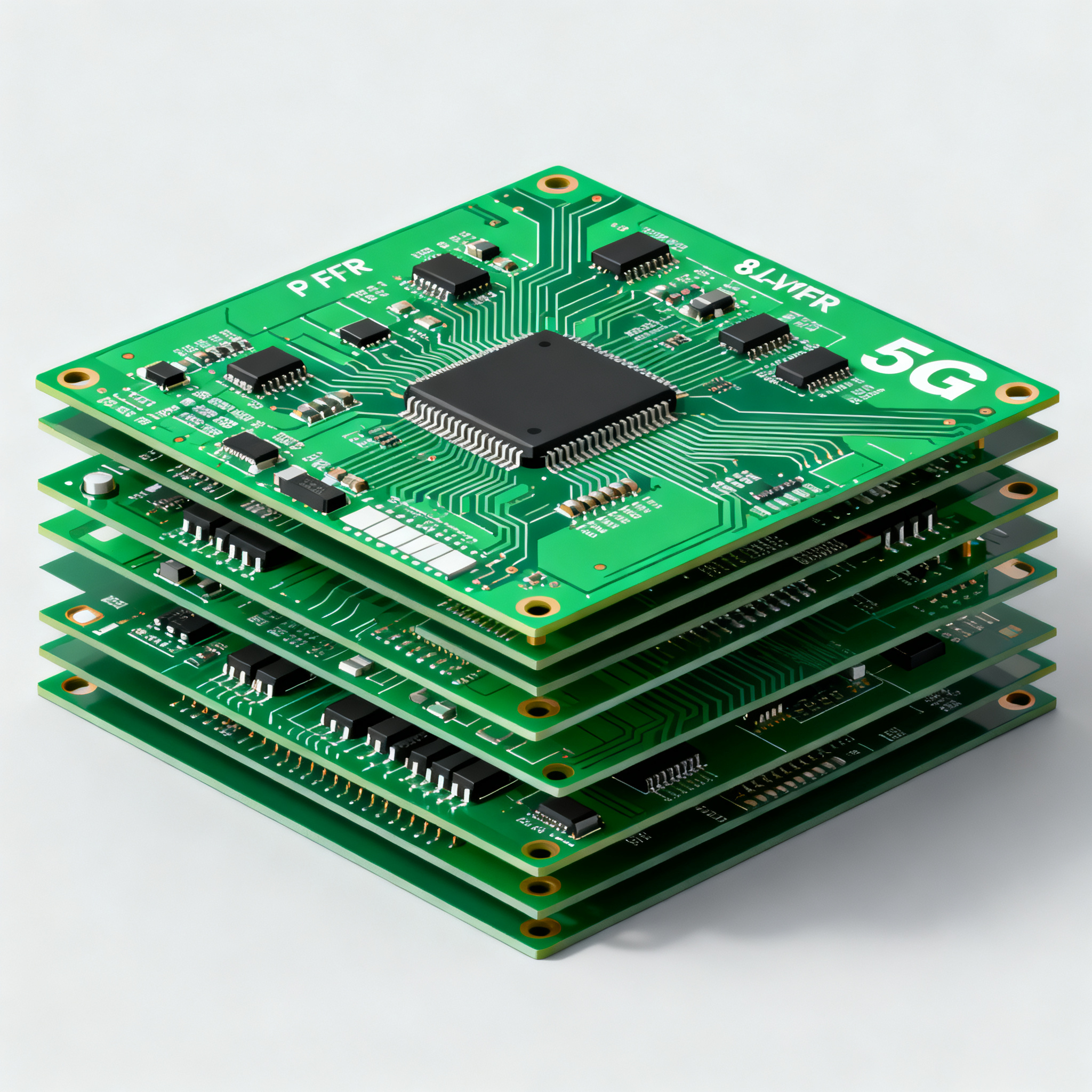
Cutting 5G Base Station PCB Assembly Costs: Material and Stackup Optimization for 8-Layer RF Boards
Why 5G Base Station PCB Costs Are Under Pressure — And Where 8-Layer RF Boards Fit In 5G network rollouts are entering a phase where every dollar of infrastructure spend is scrutinized. Massive MIMO r...
Why 5G Base Station PCB Costs Are Under Pressure — And Where 8-Layer RF Boards Fit In
5G network rollouts are entering a phase where every dollar of infrastructure spend is scrutinized. Massive MIMO radios and beamforming antenna units—the workhorses of sub-6 GHz and C-band deployments—demand RF printed circuit boards that combine low loss, tight impedance control, and high layer counts. An 8-layer stackup has become a de facto standard for these radios: it provides enough routing space for power distribution, digital control, and multiple RF channels while keeping the board footprint manageable. But the material cost of an all-high-frequency-laminate 8-layer board can easily eat 40–60% of the total assembly bill, putting enormous pressure on design teams to find savings without sacrificing signal integrity.
At Nova PCBA, we see this tension daily. Our high-mix RF assembly lines handle everything from prototype 8-layer beamformer boards to mid-volume production of remote radio units. The common thread is that engineers are being asked to deliver the same electrical performance they validated on expensive Rogers or Isola laminates, but at a cost structure that makes sense for tens of thousands of units. The answer, in many cases, lies in rethinking the stackup and material selection before the first prototype is ordered.
The cost drivers are not just the raw laminate price per square foot. They cascade into fabrication yield, lamination cycles, drilling precision, and assembly rework rates. A board that warps during reflow because of an asymmetrical stackup, or one that requires multiple sequential laminations to achieve buried capacitance, will erase any material savings in manufacturing scrap and debugging time. Understanding the interplay between dielectric properties, layer architecture, and assembly process is the key to cutting costs intelligently. This article gives you the practical framework to do exactly that—grounded in IPC design standards, real material data, and field experience with 8-layer RF boards for 5G base stations.
The 8-Layer RF Board Material Trade-Off: Dielectric Properties, Loss, and Price per Square Inch
RF board materials are defined by a handful of parameters that directly affect both electrical performance and fabrication cost. For 5G base stations operating at 3.5 GHz, the dominant concerns are dielectric constant (Dk) tolerance, dissipation factor (Df), thermal conductivity, and coefficient of thermal expansion (CTE). Dk determines the physical dimensions of 50-ohm traces and the phase velocity of signals; a tight Dk tolerance (±0.05 or better) is essential for consistent impedance across a panel. Df, or loss tangent, dictates how much signal power is converted to heat per unit length—a critical metric for link budget calculations. Thermal conductivity matters because power amplifier stages and active antenna elements can generate significant heat, and the board itself must help spread that heat to avoid hot spots. CTE, particularly in the z-axis, influences plated through-hole reliability during thermal cycling.
High-frequency laminates like Rogers RO4350B, Isola Astra MT77, and Taconic RF-35 excel in these areas but come at a premium. Meanwhile, advanced FR-4 grades—such as high-Tg, low-Dk variants—have improved to the point where they can serve as inner-layer cores in hybrid designs. The table below compares typical properties and relative cost indices for materials commonly considered in 8-layer 5G RF boards. Cost indices are normalized to a baseline FR-4 (index = 1.0) and reflect industry pricing patterns for standard thicknesses.
| Material | Dk @ 10 GHz (typical) | Df @ 10 GHz (typical) | Z-axis CTE (ppm/°C) | Thermal Conductivity (W/m·K) | Relative Cost Index (FR-4 = 1.0) |
|---|---|---|---|---|---|
| Rogers RO4350B | 3.48 ± 0.05 | 0.0037 | 35 | 0.69 | 5.0 – 7.0 |
| Isola Astra MT77 | 3.00 ± 0.04 | 0.0017 | 28 | 0.60 | 6.0 – 8.0 |
| Taconic RF-35 | 3.50 ± 0.05 | 0.0018 | 34 | 0.62 | 4.5 – 6.5 |
| High-Tg FR-4 (e.g., Isola 370HR) | 3.92 ± 0.15 | 0.0200 | 45 | 0.40 | 1.0 |
| Low-Dk FR-4 (specialty) | 3.70 ± 0.10 | 0.0100 | 40 | 0.45 | 1.2 – 1.5 |
Key Takeaway: The loss tangent of a high-frequency laminate can be an order of magnitude lower than that of standard FR-4. For 5G NR signals at 3.5 GHz, a 10-inch microstrip trace on RO4350B might exhibit around 0.15 dB of insertion loss, while the same trace on FR-4 could exceed 1.0 dB—enough to violate a tight link budget. However, not every layer carries long RF traces. By reserving expensive low-loss materials only for the layers that actually need them, you can slash the laminate bill while preserving system performance.
IPC-2221, the generic standard on printed board design, provides essential guidance on layer thickness and impedance control. It recommends that dielectric thickness between a signal layer and its reference plane be chosen to achieve the target impedance with a manufacturable trace width. For 50-ohm microstrip on a 10-mil RO4350B substrate, the trace width is about 18 mils—well within standard etching capabilities. When you substitute a lower-cost material with a higher Dk, the trace narrows, potentially increasing conductor loss and etching sensitivity. The standard also advises symmetrical construction to minimize warpage, a point we’ll return to in the guidance section. For a deeper dive, refer to IPC’s design standards and your fabricator’s specific capability data.
Hybrid vs. All-RF Laminate Stackups: A Side-by-Side Cost-Performance Analysis for 8-Layer Designs
Once you’ve selected candidate materials, the next decision is how to arrange them. Three stackup strategies dominate 8-layer RF board design for 5G base stations: an all-high-frequency-laminate construction, a hybrid that pairs RF outer layers with FR-4 inner cores, and an all-FR-4 approach with aggressive design rules. Each has a distinct cost-performance profile, and the right choice depends on your trace lengths, frequency plan, and production volume.
The comparison table below assumes a typical 8-layer board with layers 1 and 8 as RF microstrip, layers 2 and 7 as ground planes, and layers 3–6 for power and digital routing. Insertion loss is measured for a 6-inch microstrip at 3.5 GHz. Impedance tolerance reflects achievable ±% with standard etching and lamination processes. Fabrication yield is a relative indicator based on the complexity of lamination and drilling.
| Metric | All-RF Laminate (e.g., RO4350B throughout) | Hybrid (RF outer + FR-4 inner) | All-FR-4 (low-Dk grade) | Selection Criteria & Failure Boundary |
|---|---|---|---|---|
| Material cost (relative) | 5.0 – 7.0× | 1.8 – 2.5× | 1.0 – 1.3× | Hybrid cuts 25–40% vs. all-RF; all-FR-4 only viable for very short RF paths. |
| Insertion loss @ 3.5 GHz (6-inch microstrip) | 0.10 – 0.15 dB | 0.12 – 0.18 dB | 0.8 – 1.2 dB | Link budget: if total loss budget is <1 dB, all-FR-4 fails; hybrid stays within margin. |
| Impedance tolerance (50 Ω) | ±7% | ±10% | ±12–15% | Hybrid’s tolerance depends on prepreg thickness control; IPC-2221 recommends ±10% for RF. |
| PCB fab yield (relative) | High (mature process) | Medium-high (mixed materials need careful press cycles) | High (standard FR-4 process) | Hybrid requires compatible resin systems to avoid delamination; choose prepregs with similar cure temperatures. |
| Thermal management | Moderate (0.6–0.7 W/m·K) | Moderate (inner FR-4 limits heat spreading) | Low (0.4 W/m·K) | For high-power PA stages, add thermal vias or metal-core layers; hybrid may need extra thermal design. |
In practice, the hybrid stackup has become the sweet spot for many 5G radio designs. By placing the RF signal layers on Rogers RO4350B or Isola Astra MT77 and using a low-cost, high-Tg FR-4 for the inner power and digital planes, you retain nearly all the electrical performance of a full-RF board while cutting laminate costs by 25–40%. The key is to ensure that the reference plane directly adjacent to each RF trace is also a low-loss material—typically the first inner ground layer. Once the RF fields are confined between the top microstrip and that ground plane, the lossy FR-4 cores further down in the stack have negligible effect on the 50-ohm impedance or insertion loss.
All-FR-4 designs, even with specialty low-Dk grades, struggle to meet the link budgets of typical 5G base stations where trace lengths can exceed 4 inches. They may be acceptable for very compact, short-reach interconnects inside a shielded module, but for the main radio board, the insertion loss penalty is usually too high. The hybrid approach gives you the best of both worlds: RF performance that satisfies system requirements and a bill of materials that satisfies the procurement team.
Stackup and Material Selection Tactics That Trim Assembly Costs Without Compromising RF Performance
Material cost is only part of the equation. The way you configure the stackup directly influences assembly yield, rework rates, and the number of manufacturing steps. A few deliberate choices can reduce total assembly cost by 15–25% on top of the laminate savings.
1. Symmetrical stackups prevent warpage. An 8-layer board with an asymmetrical distribution of copper and dielectric will bow during reflow soldering, causing opens, shorts, and coplanarity issues with large BGA packages. Always mirror layer types and copper weights around the centerline. For a hybrid board, that means if layers 1–2 use RF laminate, layers 7–8 should too, even if layer 8 is a ground plane. This symmetry eliminates the need for costly rework and improves first-pass yield. IPC-2221 Section 5.2.4 provides explicit recommendations on symmetrical construction.
2. Standard-thickness prepregs reduce lead times and cost. Custom or non-stock prepreg thicknesses often require special orders and can delay fabrication. Stick to commonly available glass styles (e.g., 106, 1080, 2116) and resin contents that your fabricator stocks. For a hybrid stackup, choose prepregs that are compatible with both the RF laminate and the FR-4 core—your fabricator can advise on the best combination to avoid mixed-resin issues during lamination.
3. Reduce RF layer count via buried capacitance. If your design dedicates entire layers to power-to-ground capacitance for decoupling, consider using a thin buried capacitance laminate (e.g., 2 mil thick with high Dk) between the power and ground planes on inner layers. This can eliminate the need for an extra RF layer pair, reducing the total layer count or freeing up layers for other signals. Fewer RF layers mean less expensive laminate and fewer lamination cycles.
4. Partner with an assembly house that offers early DFM feedback. At Nova PCBA, we review stackup proposals before fabrication begins, checking for impedance feasibility, material compatibility, and assembly process risks. A 30-minute design review can prevent a $20,000 prototype run from being scrapped due to an unmanufacturable prepreg combination or an impedance mismatch that only surfaces during testing. Early collaboration also helps you specify the right copper weights and surface finishes for both RF performance and assembly robustness.
The table below summarizes common stackup parameters and their cost impact for an 8-layer hybrid RF board. Use it as a checklist when finalizing your design.
| Parameter | Typical Low-Cost Choice | Impact on Assembly Cost | Notes |
|---|---|---|---|
| Copper weight on RF layers | ½ oz (18 µm) | Thinner copper reduces etching cost and improves fine-line yield; adequate for signal traces. | Use 1 oz for ground/power planes if thermal demands require it. |
| Dielectric thickness (RF trace to reference plane) | 10 mil (254 µm) for 50 Ω on RO4350B | Standard thickness avoids custom prepregs; thicker dielectrics increase trace width, lowering conductor loss. | Confirm impedance with a field solver; IPC-2221 provides initial guidance. |
| Prepreg type | 1080 or 2116 glass, standard resin | Stock materials keep fabrication cost low and lead times short. | Ensure resin system matches both RF and FR-4 laminates. |
| Lamination cycles | Single lamination for 8-layer | Multiple cycles add 15–25% to PCB cost and risk registration errors. | Design all layers to be pressed in one cycle; avoid sequential laminations unless absolutely necessary. |
| Surface finish | ENIG (electroless nickel immersion gold) | Good for RF and assembly; immersion silver is an alternative but requires careful handling. | HASL is not recommended for fine-pitch RF due to uneven surfaces. |
| Impedance test coupons | Include on production panel | Adds minimal cost but verifies Dk and impedance before assembly, preventing expensive rework. | Work with fabricator to design coupons that reflect actual trace geometries. |
Tip: Before freezing the stackup, run a 3D electromagnetic simulation of the entire signal path—including launches, vias, and connectors—using the exact material properties from the laminate supplier’s datasheet. A small impedance discontinuity at a via can create return loss that eats into your hard-won margin. Many engineers also order a small pilot run with impedance coupons and perform vector network analyzer (VNA) measurements to correlate simulation with reality. This step pays for itself many times over when you avoid a field failure in a 5G base station.
Your Toughest Questions About Cost-Effective 8-Layer RF PCB Assembly, Answered
Q: How much cost can I realistically save by switching from an all-Rogers 8-layer board to a hybrid FR-4/Rogers stackup?
A: Material costs can drop 25–40% because high-frequency laminates are 5–10× more expensive than advanced FR-4. The exact saving depends on layer count and board size, but a hybrid approach typically retains 90% of the RF performance while cutting the laminate bill significantly. For example, if an all-RO4350B 8-layer board costs $120 in laminate per square foot, a hybrid with RO4350B on layers 1–2 and 7–8 and FR-4 inner cores might cost $70–$85. The savings multiply in production volumes of 5,000 units or more.
Q: What key IPC-2221 guidelines must I follow for an 8-layer RF stackup to avoid signal integrity issues when using lower-cost materials?
A: IPC-2221 provides rules for controlled impedance, trace width/spacing, and dielectric thickness. For hybrid boards, maintain consistent reference planes, keep RF traces on the outermost high-performance layers, and verify that the prepreg thickness between RF layers and adjacent ground planes meets the target impedance tolerance (±10%). The standard also recommends symmetrical construction to minimize warpage and advises that the dielectric material directly adjacent to a controlled-impedance trace be specified with a known Dk and thickness. Always cross-check your stackup with a field solver and your fabricator’s process capabilities.
Q: Can I use standard FR-4 for inner layers and still achieve reliable 50-ohm impedance control on the outer RF layers?
A: Yes, if the outer RF layers are a low-loss laminate and the FR-4 inner cores are used only for power and digital routing. The critical factor is the dielectric spacing between the RF trace and its reference plane; as long as that is a stable, low-Dk material, the inner FR-4 layers do not directly degrade the outer impedance. The electromagnetic field of a microstrip is concentrated between the trace and the first ground plane. So if layers 1 (RF) and 2 (ground) are both Rogers material, the FR-4 starting at layer 3 has negligible effect on the 50-ohm impedance of the top trace.
Q: What is the minimum copper weight and dielectric thickness I can specify to reduce material cost without risking manufacturability?
A: For 8-layer RF boards, ½ oz (18 µm) copper on signal layers and 3–4 mil (75–100 µm) core/prepreg thicknesses are common. Going thinner increases the risk of etching defects and handling damage. Always consult your fabricator’s capability limits and run a DFM check; Nova PCBA can help validate these choices early. Thinner dielectrics also increase capacitance and can lower impedance, so you may need to narrow trace widths, which in turn raises conductor loss. Balance cost savings with electrical and mechanical robustness.
Q: How do I verify that a cost-optimized stackup meets 5G NR phase noise and return loss requirements before committing to production?
A: Perform 3D electromagnetic simulation of the exact stackup and run a small pilot build with impedance coupons and vector network analyzer measurements. Compare S-parameter results against your system link budget. Many engineers also use test coupons on the production panel to confirm Dk and loss tangent of the actual laminates used. This correlation step is critical because laminate suppliers’ datasheet values are typical; your specific batch may vary slightly. A pilot run of 10–20 boards with full RF testing gives you the confidence to release the design to volume production.
References & Further Reading
- IPC — PCB Design and Manufacturing Standards (IPC-2221, IPC-A-610)
- Nova PCBA — Professional PCB Assembly Services
- Rogers Corporation — RO4000 Series High Frequency Laminates
- Isola — Astra MT77 Low Loss Laminate
- AGC Multi Material (Taconic) — RF-35 Laminate
- Isola — 370HR High-Tg FR-4
- Signal Integrity Journal — Hybrid PCB Stackup Design for RF and Digital Systems
- Microwave Journal — Comparing PCB Materials for 5G Applications
Optimizing the cost of an 8-layer RF board for 5G base stations is a multi-dimensional challenge that starts with material selection and stackup architecture. By adopting a hybrid approach, enforcing symmetry, and collaborating early with your assembly partner, you can deliver boards that meet stringent RF specifications at a cost structure that supports large-scale deployment. The techniques outlined here—grounded in IPC standards and real-world fabrication experience—give you a repeatable framework to balance performance and budget. For a hands-on review of your next 5G PCB design, reach out to Nova PCBA; our engineering team can help you validate your stackup, run DFM analysis, and move from prototype to production with confidence.