Custom PCB Fabrication Process: A Practical Guide with Real Examples for Tailored Solutions
Custom PCB Fabrication Process: A Practical Guide with Real Examples for Tailored Solutions Introduction In the ever-evolving landscape of electronics, custom PCB (Printed Circuit Board) fabrication p...
Introduction
In the ever-evolving landscape of electronics, custom PCB (Printed Circuit Board) fabrication plays a pivotal role in creating tailored solutions for unique applications. As the backbone of electronic devices, PCBs are crucial for the effective functioning of integrated circuits (ICs) and other components. In this guide, we delve into the intricacies of the custom PCB fabrication process, focusing on component specifications, datasheets, selection criteria, and application circuits. Whether you're designing for consumer electronics, industrial applications, or cutting-edge technology, understanding the nuances of PCB fabrication is essential for achieving optimal performance and reliability.
Technical Overview
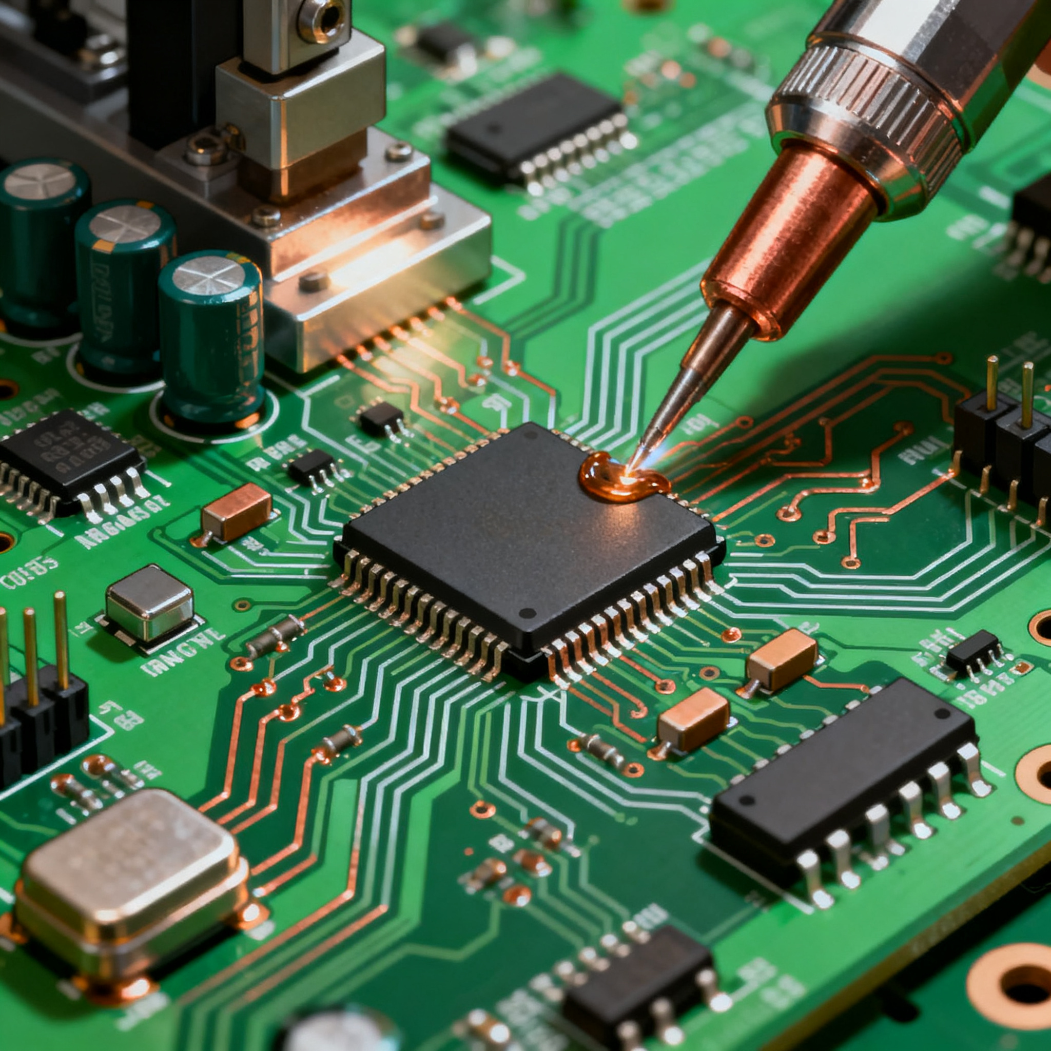
At the core of any electronic design is the PCB, which provides the structural and electrical foundation for components like ICs, resistors, capacitors, and more. Custom PCBs are designed to meet specific requirements, making them ideal for specialized applications. The architecture of a PCB involves multiple layers, including the substrate, copper traces, solder mask, and silkscreen, each serving a distinct purpose. The principles of PCB design focus on minimizing electrical noise, ensuring signal integrity, and optimizing thermal management. By adhering to industry standards such as those set by the IPC, engineers can ensure high-quality and reliable PCB designs.
In custom PCB fabrication, selecting the right components is crucial. This involves understanding the specifications and datasheets of IC chips, which provide detailed information on performance metrics, electrical characteristics, and packaging. By analyzing these specifications, engineers can make informed decisions about component selection, ensuring compatibility and functionality within the overall design.
Detailed Specifications
Component specifications are vital in the PCB design process as they dictate the performance and capabilities of the final product. Understanding these specifications allows engineers to select components that meet the required operational parameters and ensure seamless integration within the PCB. Key specifications include CPU speed, memory, peripherals, power requirements, and package type. These factors influence the overall efficiency, size, and cost of the PCB.
| Specification | Description | Example Value |
|---|---|---|
| CPU Speed | Clock speed of the central processing unit | 1.2 GHz |
| Memory | Amount of RAM available | 512 MB |
| Peripherals | Supported peripheral interfaces | USB, I2C, SPI |
| Power Supply | Operating voltage range | 3.3V - 5V |
| Package Type | Physical form factor of the IC | QFP |
| Operating Temperature | Temperature range for operation | -40°C to 85°C |
| Storage Temperature | Temperature range for storage | -55°C to 125°C |
| ESD Protection | Electrostatic discharge protection level | ±2 kV |
| MTBF | Mean time between failures | 100,000 hours |
| Packaging Options | Available packaging | Tray, Reel |
Key Takeaways from the Specifications
The specifications outlined in Table 1 provide a comprehensive overview of the critical parameters that influence the performance and suitability of IC chips for custom PCB designs. CPU speed and memory are fundamental for determining the processing capability and data handling capacity of the device. Peripherals such as USB, I2C, and SPI ensure connectivity and communication with other components. The power supply range is crucial for compatibility with different power sources, while the package type affects the physical integration into the PCB. Understanding these specifications allows engineers to select components that align with the design goals and operational requirements of the project.
| Characteristic | Description | Example Value |
|---|---|---|
| Supply Voltage | Voltage required for operation | 3.3V |
| Supply Current | Current consumption during operation | 50 mA |
| Input Voltage Range | Acceptable input voltage levels | 0V to 3.6V |
| Output Voltage | Voltage level at output pins | 3.3V |
| Output Current | Current provided at output pins | 20 mA |
| Propagation Delay | Time taken for signal propagation | 5 ns |
| Rise Time | Time taken for signal to rise from low to high | 2 ns |
| Fall Time | Time taken for signal to fall from high to low | 2 ns |
| Input Capacitance | Capacitance at input pins | 5 pF |
| Output Capacitance | Capacitance at output pins | 10 pF |
| Thermal Resistance | Resistance to heat flow | 50 °C/W |
Practical Implications
The electrical characteristics detailed in Table 2 are crucial for ensuring the reliable operation of IC chips within a PCB. Supply voltage and current are fundamental parameters that determine the power requirements of the chip. Input and output voltage levels are critical for interfacing with other components, while propagation delay, rise time, and fall time affect the speed and accuracy of signal processing. Input and output capacitance influence the loading effects and signal integrity. Thermal resistance is essential for managing heat dissipation and preventing overheating. By understanding these characteristics, engineers can design PCBs that optimize performance and ensure long-term reliability.
| Use Case | Configuration | Example Application |
|---|---|---|
| Consumer Electronics | High-speed, low power | Smartphones, Tablets |
| Industrial Automation | Robust, high power | Control Systems, PLCs |
| Automotive | High reliability, temperature tolerant | Engine Control Units |
| Medical Devices | Precision, low noise | Diagnostic Equipment |
| Telecommunications | High frequency, wide bandwidth | Routers, Modems |
| Wearable Devices | Compact, energy-efficient | Smartwatches, Fitness Trackers |
| IoT Applications | Low power, connectivity | Smart Home Devices |
Application Guidelines
Table 3 highlights the diverse applications and configurations of IC chips within different industries. Consumer electronics demand high-speed and low-power configurations for devices like smartphones and tablets. Industrial automation requires robust and high-power configurations for reliable control systems. Automotive applications necessitate high reliability and temperature tolerance for components like engine control units. Medical devices prioritize precision and low noise for diagnostic equipment. Telecommunications benefit from high frequency and wide bandwidth for routers and modems. Wearable devices require compact and energy-efficient configurations for products like smartwatches. IoT applications emphasize low power and connectivity for smart home devices. Understanding these use cases helps engineers tailor their PCB designs to meet specific application requirements.
Design Considerations
Designing a custom PCB involves several critical considerations to ensure optimal performance and reliability. First, component placement is crucial for minimizing signal interference and ensuring efficient heat dissipation. Placing components strategically can reduce trace lengths, thereby minimizing resistance and inductance. Second, trace routing should be optimized to avoid crosstalk and signal reflections. Using differential pairs and controlled impedance can enhance signal integrity, especially in high-speed applications. Third, power distribution should be carefully designed to provide stable voltage levels across the PCB. Implementing power planes and decoupling capacitors can mitigate voltage drops and noise.
Thermal management is another vital aspect of PCB design, particularly for components that generate significant heat. Incorporating thermal vias, heat sinks, and adequate airflow can prevent overheating and extend the lifespan of the PCB. Additionally, adhering to industry standards, such as IPC guidelines, ensures that the PCB design meets quality and reliability benchmarks. By considering these factors, engineers can create custom PCBs that deliver superior performance and durability.
Step-by-Step Implementation
- Define Requirements: Begin by outlining the specific requirements and constraints of the project, including performance goals, environmental conditions, and budget.
- Select Components: Choose components based on their specifications and compatibility with the design requirements. Refer to datasheets for detailed information.
- Create Schematic: Develop a schematic diagram that represents the electrical connections between components. Use design software to ensure accuracy and completeness.
- Design PCB Layout: Translate the schematic into a PCB layout, considering component placement, trace routing, and power distribution. Utilize design rules to maintain signal integrity.
- Prototype Fabrication: Submit the design files to a PCB manufacturer for prototype fabrication. Verify that the prototype meets the design specifications and make necessary adjustments.
- Testing and Validation: Perform thorough testing to validate the functionality and performance of the prototype. Use testing equipment to measure electrical parameters and identify any issues.
- Iterate and Optimize: Based on test results, refine the design to address any shortcomings. Iterate the process to optimize performance and reliability.
- Final Production: Once the design is finalized, proceed with full-scale production. Ensure quality control measures are in place to maintain consistency and reliability.
Common Issues & Solutions
- Signal Integrity Issues: Use controlled impedance and differential pairs to minimize reflections and crosstalk in high-speed designs.
- Thermal Management Challenges: Incorporate thermal vias and heat sinks to manage heat dissipation and prevent component overheating.
- Power Distribution Problems: Implement power planes and decoupling capacitors to ensure stable voltage levels and reduce noise.
- Component Compatibility Errors: Verify component specifications and compatibility during the selection process to avoid mismatches.
- Manufacturing Defects: Conduct thorough inspections and testing to identify and rectify manufacturing defects before deployment.
- Environmental Constraints: Design for environmental conditions by selecting components with appropriate temperature and humidity ratings.
Applications & Use Cases
Custom PCBs are utilized across a wide range of applications, each with unique requirements and challenges. In consumer electronics, custom PCBs enable the creation of compact and efficient devices such as smartphones and tablets. In industrial automation, they provide robust and reliable solutions for control systems and automation equipment. Automotive applications benefit from custom PCBs designed for high reliability and temperature tolerance, essential for engine control units and safety systems. Medical devices utilize custom PCBs for precision and low noise, crucial for diagnostic equipment and patient monitoring systems. Telecommunications rely on custom PCBs for high frequency and bandwidth, supporting the infrastructure of routers and modems.
Selection & Sourcing Guide
When selecting and sourcing components for custom PCBs, it's essential to consider factors such as performance, compatibility, and availability. Utilize resources like IC Online to access a wide range of components and datasheets. Evaluate suppliers based on their reputation, lead times, and pricing to ensure reliable and cost-effective sourcing. Additionally, consider the availability of technical support and documentation to assist in the design and troubleshooting processes. By carefully selecting and sourcing components, engineers can create custom PCBs that meet the desired specifications and deliver exceptional performance.
FAQ
- What is the importance of component specifications in PCB design? Component specifications dictate the performance and capabilities of the PCB, ensuring compatibility and functionality within the design.
- How do I select the right IC chip for my PCB design? Analyze the datasheet for performance metrics, electrical characteristics, and packaging to ensure compatibility with your design requirements.
- What are the key considerations for PCB layout design? Focus on component placement, trace routing, power distribution, and thermal management to optimize performance and reliability.
- How can I ensure signal integrity in my PCB design? Use controlled impedance, differential pairs, and proper trace routing to minimize reflections and crosstalk.
- What are the common challenges in custom PCB fabrication? Signal integrity issues, thermal management, power distribution, and manufacturing defects are common challenges that require careful design and testing.
- How do I manage thermal dissipation in a PCB? Incorporate thermal vias, heat sinks, and adequate airflow to prevent overheating and ensure reliable operation.
- What is the role of IPC standards in PCB design? IPC standards provide guidelines for design, assembly, and quality inspection, ensuring high-quality and reliable PCBs.
- How can I test and validate my PCB prototype? Use testing equipment to measure electrical parameters and perform thorough inspections to validate functionality and performance.
- What are the benefits of custom PCBs in consumer electronics? Custom PCBs enable compact and efficient designs, supporting the development of advanced consumer electronics like smartphones and tablets.
- How do I handle component shortages during sourcing? Identify alternative suppliers and consider substitute components that meet the required specifications and availability.
Conclusion
Custom PCB fabrication is a critical process in the development of tailored solutions for various applications. By understanding component specifications, electrical characteristics, and application requirements, engineers can design PCBs that deliver optimal performance and reliability. Through careful selection, sourcing, and design considerations, custom PCBs can meet the unique demands of industries ranging from consumer electronics to industrial automation. As technology continues to advance, the role of custom PCBs will remain pivotal in driving innovation and enabling the next generation of electronic devices.