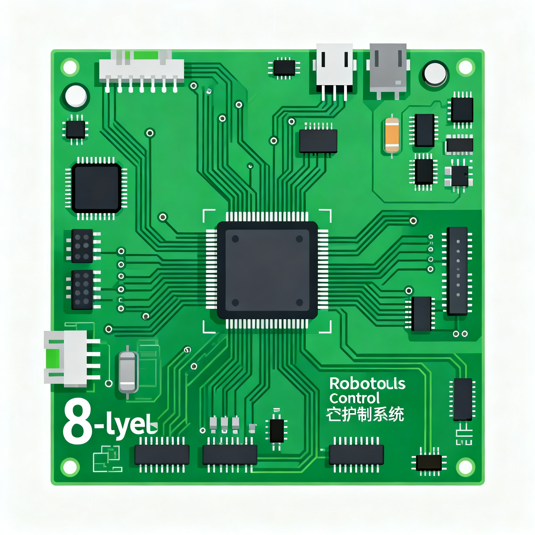
Cost Optimization Tips for 8-Layer Robotics Control System PCB Assembly: Balancing High-Speed Design and Thermal Management
Cost Optimization Tips for 8-Layer Robotics Control System PCB Assembly: Balancing High-Speed Design and Thermal Management Why 8-Layer Robotics Control Boards Are Pushing Cost Boundaries Right Now Mo...
Cost Optimization Tips for 8-Layer Robotics Control System PCB Assembly: Balancing High-Speed Design and Thermal Management
Why 8-Layer Robotics Control Boards Are Pushing Cost Boundaries Right Now
Modern robotics control systems are no longer simple microcontroller boards. They combine high-speed digital interfaces like EtherCAT, CAN FD, and SPI with precision analog feedback from encoders, torque sensors, and motor current shunts, all while switching power stages that can dump 50 W or more into the board. The result is a dense, mixed-signal environment where signal integrity and thermal management collide. An 8-layer stack-up has become the practical baseline for routing these functions without sacrificing performance, but it also puts procurement teams under intense cost pressure. You need a board that works first time in the field—downtime on a production robot can cost thousands per hour—yet you cannot let the bare PCB and assembly costs spiral out of control.
This tension is real. The IPC-2221 design standard gives you a framework for impedance control, creepage, and thermal management, but it does not tell you how to shave 15% off the unit price. That requires a deep understanding of how layer arrangement, via technology, and material selection interact with both signal quality and heat flow. It also demands an assembly partner that can provide early DFM feedback and understands that high-reliability manufacturing does not have to mean over‑specification. At Nova PCBA, we routinely help robotics teams navigate these trade-offs, balancing performance with cost from prototype through volume production. In this article, I’ll walk you through the stack-up physics, the real cost drivers hidden in your design choices, and the concrete moves that cut assembly costs without compromising the control loop.
Inside the 8-Layer Stack-Up: How Layer Arrangement Dictates Signal Quality and Heat Flow
Before you can optimize cost, you need to understand what an 8-layer board does for you electrically and thermally. In a robotics controller, the stack-up is not just a routing convenience—it directly sets the impedance environment for high-speed traces, determines crosstalk between digital and analog sections, and creates the thermal path from hot components to the ambient air or a heatsink. The most common configuration places signal layers on the outer surfaces and buries power and ground planes inside, but small variations in the order of those planes can dramatically change both signal integrity and heat spreading.
Consider the classic symmetric stripline stack: Sig/GND/PWR/Sig/Sig/PWR/GND/Sig. Here, the two inner signal layers are sandwiched between power and ground planes, providing excellent shielding and controlled impedance. The outer signal layers can be microstrip, but they are often used for lower-speed signals or component fanout. This arrangement keeps high-speed buses on the inner stripline layers, where via stubs are minimal if you route from top to an inner layer and stop there. For thermal management, the solid ground and power planes act as heat spreaders, moving heat away from hot spots toward the board edges or thermal vias. However, if you need to isolate analog and digital grounds or run multiple power rails, you may need a dual stripline stack: Sig/GND/Sig/PWR/GND/Sig/GND/Sig. This adds extra ground planes, which improves crosstalk isolation but increases the layer count and material cost.
A mixed microstrip approach—where you keep one or two outer layers as microstrip for critical high-speed signals and use inner layers for power and ground—can reduce layer transitions and via stubs for those signals, but it often complicates the return path and can increase EMI if not carefully designed. The table below compares three practical 8-layer stack-ups across the metrics that matter most for robotics control boards.
| Stack-Up Configuration | Typical Impedance Tolerance | Via Stub Risk | Effective Copper Weight for Heat Spreading | Crosstalk (Adjacent Signal Layers) | Relative Cost Impact |
|---|---|---|---|---|---|
| Symmetric Stripline (Sig/GND/PWR/Sig/Sig/PWR/GND/Sig) | ±10% (50 Ω single-ended, 100 Ω differential) | Low – high-speed signals routed on inner stripline layers, vias can be back-drilled if needed | 1 oz (35 µm) on planes, 0.5 oz on signal layers | −40 dB at 1 GHz | Baseline (standard 8-layer) |
| Dual Stripline (Sig/GND/Sig/PWR/GND/Sig/GND/Sig) | ±8% – better isolation allows tighter control | Moderate – more layer transitions, but ground planes shield stubs | 1 oz on all plane layers, improved lateral spreading | −50 dB at 1 GHz | +5–10% (extra ground planes increase material and processing) |
| Mixed Microstrip (Sig/GND/PWR/Sig/GND/Sig/PWR/Sig) | ±10% on outer microstrip, ±12% on inner stripline | High on outer layers if vias pass through entire board; requires careful via design | 1 oz on planes; outer layers can be 1 oz for direct heat sinking | −35 dB (outer microstrip couples more easily) | Comparable to symmetric, but may need extra shielding |
Tip: The symmetric stripline configuration is the workhorse for most robotics controllers. It gives you four routing layers (two outer, two inner) with solid reference planes, and the inner stripline layers are ideal for DDR memory buses or high-speed serial links. By keeping the high-speed signals on the inner layers, you eliminate the need for exotic low-loss laminates—standard high-Tg FR-4 is often sufficient up to several GHz, as long as you manage trace lengths and via stubs. The dual stripline stack is overkill unless you have extremely sensitive analog front-ends that must be shielded from digital noise, or you are running multiple independent power domains that require dedicated ground planes. The mixed microstrip approach can be useful when you need to place a heatsink directly on outer-layer copper pours, but it demands more careful EMI control. In all cases, the right stack-up choice can avoid the cost of moving to 10 or 12 layers, or the premium of high-frequency laminates like Rogers 4350B, saving you 20–30% on bare board cost.
Stack-Up, Via, and Material Choices: Where the Real Cost Trade-Offs Hide
Once you have a stack-up architecture, the next layer of cost optimization lives in the details: via technology, substrate material, and surface finish. These three elements interact strongly. For example, a dense BGA with 0.8 mm pitch may force you into microvias, which then drives up the board cost and may require a high-Tg laminate to survive multiple lamination cycles. Conversely, a thoughtful fanout and layer assignment can keep you in through-hole vias, letting you use a standard FR-4 material and an economical surface finish. The table below maps the trade-offs for the most common options in robotics control boards.
| Design Element | Option A (Lowest Cost) | Option B (Balanced) | Option C (Highest Performance) | Selection Criteria & Cost Impact |
|---|---|---|---|---|
| Via Type | Through-hole vias only | Blind vias (1-2 layers) + through-hole | Stacked microvias + buried vias | Through-hole adds stub capacitance but costs least. Blind vias add one lamination cycle (+10–15%). Microvias require multiple laminations and laser drilling (+25–40% bare board cost). Use only when escape routing from 0.5 mm-pitch BGAs leaves no alternative. |
| Substrate Material | Standard FR-4 (Tg 130°C) | High-Tg FR-4 (Tg 170°C) | Metal-core (aluminum) or polyimide | Standard FR-4 works for ambient temperatures below 85°C and moderate power. High-Tg FR-4 adds ~5–10% material cost but handles lead-free soldering and higher operating temps reliably. Metal-core is 2–3× the cost and limits to 1-2 layers; reserve for extreme thermal density. |
| Surface Finish | HASL (lead-free) | Immersion Silver or OSP | ENIG (electroless nickel immersion gold) | HASL is cheapest but uneven—avoid for fine-pitch components. Immersion silver and OSP are flat, cost ~10–15% more than HASL, and suit most robotics boards. ENIG adds ~20–30% over immersion silver but provides excellent shelf life and coplanarity, reducing assembly defects in vibration-prone environments. |
Many robotics control boards do not need IPC Class 3 acceptance. The IPC-A-610 Class 2 standard delivers the durability required for industrial robotics where occasional downtime is acceptable, while cutting inspection and rework costs significantly. Reserve Class 3 for safety-critical functions like collaborative robot force limiting or surgical robotics. Over-specifying the inspection class can add 15–25% to assembly cost without a corresponding reliability gain. Similarly, selecting ENIG when immersion silver would suffice can inflate the BOM by a few dollars per board—a figure that multiplies quickly in volume. The key is to match each choice to the actual operating environment, not to a hypothetical worst-case scenario.
Design Moves That Cut Assembly Costs Without Sacrificing Performance
Cost optimization is not a single decision; it’s a series of small, deliberate moves that accumulate into double-digit savings. The following table captures the most impactful design actions and their typical cost reduction potential when applied to an 8-layer robotics control board.
| Design Move | Cost Reduction Potential | How It Works | Implementation Notes |
|---|---|---|---|
| Merge power planes and use careful decoupling | 5–10% (can eliminate one layer) | Combine multiple voltage rails on a single split plane, using decoupling capacitors and ferrite beads to isolate noise. This may allow a 6-layer design instead of 8. | Verify power integrity with simulation; ensure split planes do not cross high-speed return paths. |
| Optimize via count and fanout patterns | 3–7% (fewer drills, less plating) | Use dog-bone fanout for BGAs, share vias for ground connections, and avoid unnecessary stitching vias. | Maintain adequate ground via density for thermal and return current; do not starve the planes. |
| Maximize panel utilization | 10–15% per board | Design rectangular board outlines, avoid internal cutouts, and fit multiple boards on a standard 18×24″ panel. Work with fabricator on array layout early. | Even a 5 mm reduction in board width can increase panel yield from 70% to 90%. |
| Choose standard laminate thicknesses and copper weights | 5–8% (material and lead time) | Stick to 0.062″ (1.6 mm) total thickness and 1 oz copper on planes, 0.5 oz on signals. Custom thicknesses require special prepregs and increase NRE. | If you need thicker copper for high current, use 2 oz on outer layers only and keep inner planes at 1 oz. |
| Avoid buried vias unless density demands them | 20–40% (bare board cost) | Buried vias add lamination cycles and precision drilling. Use through-hole vias with back-drilling if stubs are problematic, or a single microvia layer for BGA escape. | Back-drilling adds ~5–10% over through-hole, far less than buried vias. |
| Specify surface finish that matches shelf life and soldering process | 10–20% (finish cost) | Immersion silver or OSP for fine-pitch components; ENIG only if long shelf life or flatness is critical. | OSP requires careful handling to avoid oxidation; immersion silver offers a good balance. |
Beyond these moves, engage your assembly partner early. At Nova PCBA, we provide DFM (Design for Manufacturability) feedback that catches issues like insufficient solder mask dams, tombstoning risks, or thermal relief problems before they become rework costs. Our experience with robotics control boards means we can spot over-specification—for example, a 4-mil trace/space requirement when 5 mil would work, which can reduce fabrication yield and increase cost. We also help you align your design with IPC-A-610 Class 2 acceptance criteria, ensuring that quality targets are met without unnecessary inspection overhead. A well-executed DFM cycle can reduce assembly defects by 30–50%, directly lowering the total cost of ownership.
Robotics Control PCB Cost Questions Engineers and Buyers Actually Ask
Q: How do I decide between a standard 8-layer stack-up and a custom one for my robotics controller?
A: Start with a proven standard stack-up from your fabricator, such as the symmetric stripline configuration described earlier. Most established PCB manufacturers have qualified stack-ups with known impedance and material properties. Custom stack-ups add NRE (non-recurring engineering) charges and lead time because the fabricator must test and validate the new prepreg and core combinations. Only justify a custom stack-up if your design has unique impedance targets—for example, a 40 Ω single-ended requirement for a specific DDR interface—or extreme thermal requirements that cannot be met by adjusting trace geometry and copper weight on a standard build. In nine out of ten robotics controllers, a standard stack-up with careful trace tuning will meet all signal integrity goals while keeping costs predictable.
Q: What's the typical cost adder for buried vias in an 8-layer board?
A: Buried vias require additional lamination cycles and precision drilling, often increasing bare board cost by 20–40% compared to a through-hole-only design. The exact adder depends on the number of buried via layers and the fabricator’s capabilities. Use buried vias only when escape routing from high-pin-count BGAs (0.5 mm pitch or finer) leaves no alternative. In many cases, you can optimize fanout and layer assignment to stay with through-hole vias or a single microvia layer on the outer surfaces, which adds only 10–15% to the board cost. If via stubs are the concern, consider back-drilling, which is significantly cheaper than buried vias and eliminates the stub capacitance that degrades high-speed signals.
Q: Can I use standard FR-4 for high-speed digital and still manage thermal in a robotics control board?
A: Yes, if you select a high-Tg FR-4 (170°C or higher) and use thermal vias, copper pours, and adequate plane thickness. For most robotics applications without extreme ambient temperatures (above 85°C), high-Tg FR-4 avoids the cost of polyimide or metal-core laminates. The key is to verify that the operating temperature and total power dissipation stay within the material’s safe range. Use thermal simulation to identify hot spots, then add an array of thermal vias under power components to conduct heat into the internal ground planes. A 1 oz solid ground plane can spread heat effectively, and adding a heatsink to the outer copper pour further reduces junction temperatures. This approach keeps the material cost low while meeting the thermal demands of motor drivers and processors.
Q: Which surface finish minimizes cost while ensuring reliability for robotics control assemblies?
A: Immersion silver and OSP (Organic Solderability Preservative) are often the most economical for fine-pitch components and offer good solderability. Immersion silver provides a flat surface and handles multiple reflow cycles well, making it suitable for double-sided assemblies. OSP is slightly cheaper but has a shorter shelf life and requires careful handling to prevent oxidation. ENIG (Electroless Nickel Immersion Gold) provides better shelf life and excellent coplanarity, which can reduce assembly defects in boards that experience vibration—a common condition in robotics. The slight premium for ENIG (typically 20–30% over immersion silver) is often justified when you consider the total cost of rework and field failures. For high-volume industrial robots where vibration is moderate, immersion silver strikes a good balance.
Q: How does panel utilization affect per-board cost for 8-layer PCBs?
A: Panel utilization directly impacts material waste and process efficiency. Designing boards with rectangular shapes, avoiding internal cutouts, and using standard panel sizes (e.g., 18×24 inches) can improve utilization from 70% to over 90%, reducing per-unit cost by 10–15%. For example, if your board is 100×80 mm, a panel might fit 20 boards at 70% utilization, but a slight redesign to 95×75 mm could fit 24 boards, spreading the fixed processing cost over more units. Work with your fabricator early to optimize the array layout; they can suggest the best panelization strategy, including rail placement and breakaway tab design, to maximize yield without compromising assembly.
Q: What IPC class should I target for robotics control boards to balance cost and reliability?
A: IPC Class 2 is typically sufficient for industrial robotics where occasional downtime is acceptable. Class 2 allows for some visual imperfections and less stringent inspection criteria, which reduces inspection time and rework costs significantly—often by 15–25% compared to Class 3. Reserve Class 3 for safety-critical or life-support functions, such as force-limited collaborative robots or surgical systems. Most robotics control boards operate in controlled environments with scheduled maintenance, so Class 2 meets the durability needs while keeping assembly costs in check. Always confirm with your end customer or regulatory body, but do not default to Class 3 out of habit.
Balancing high-speed design and thermal management in an 8-layer robotics control board does not have to break the budget. The stack-up you choose, the via technology you permit, and the materials you specify all interact to determine both performance and cost. By starting with a standard symmetric stripline configuration, using through-hole vias wherever possible, selecting high-Tg FR-4, and matching the surface finish to the real operating environment, you can often achieve the required signal integrity and thermal performance without exotic materials or unnecessary layers. Engaging an assembly partner like Nova PCBA early in the design cycle adds a layer of practical DFM insight that catches over-specification and manufacturability issues before they inflate the BOM. The result is a reliable robotics controller that meets both your engineering targets and your cost targets, from prototype through volume production.
References & Further Reading
- IPC-2221: Generic Standard on Printed Board Design – Core design principles for impedance control, creepage, and thermal management.
- IPC-A-610: Acceptability of Electronic Assemblies – Defines Class 2 and Class 3 acceptance criteria for PCB assembly.
- Nova PCBA – Professional PCB Assembly Services – Turnkey assembly and DFM support for robotics control boards.
- Nova PCBA Assembly Capabilities – Detailed process capabilities and quality standards.
- PCBWay Stack-Up Design Guide – Practical stack-up examples and impedance calculation tools.
- EETimes – High-Speed PCB Design Tips – Articles on signal integrity, via design, and material selection.
- Ultra Librarian – CAD Footprints and Models – Verified component libraries that reduce design errors and rework.
- Electronics Cooling Magazine – Thermal Via Design – Research and guidelines for thermal via arrays and heat spreading in PCBs.
- Octopart – Electronic Component Search Engine – Real-time pricing and availability for BOM cost optimization.