Cost Optimization Strategies for Multilayer PCB Projects: Save on 6-Layer Designs
Cost Optimization Strategies for Multilayer PCB Projects: Save on 6-Layer Designs Introduction In the rapidly evolving electronics industry, optimizing the cost of multilayer PCB projects, particularl...
Introduction
In the rapidly evolving electronics industry, optimizing the cost of multilayer PCB projects, particularly 6-layer designs, is essential for competitive advantage. As electronic devices become more complex, the demand for efficient, high-performance PCBs at a lower cost increases. Engineers and designers are challenged to balance performance, reliability, and cost-effectiveness, making strategic decisions crucial. This article explores cost optimization strategies, focusing on circuit topology, component calculations, performance analysis, and design trade-offs to ensure high-quality, affordable PCB designs.
Technical Overview
Multilayer PCBs are integral to modern electronics, providing increased circuit density and improved performance. A 6-layer PCB design consists of six stacked layers of conductive and insulating materials, allowing for complex circuit configurations. Key concepts such as circuit topology, which involves the arrangement and connection of components, play a critical role in determining the overall performance and cost of the PCB. Understanding the principles of component calculations and performance analysis is vital for optimizing design efficiency. By adhering to industry standards like those outlined by IPC, designers can ensure quality and reliability while minimizing costs.
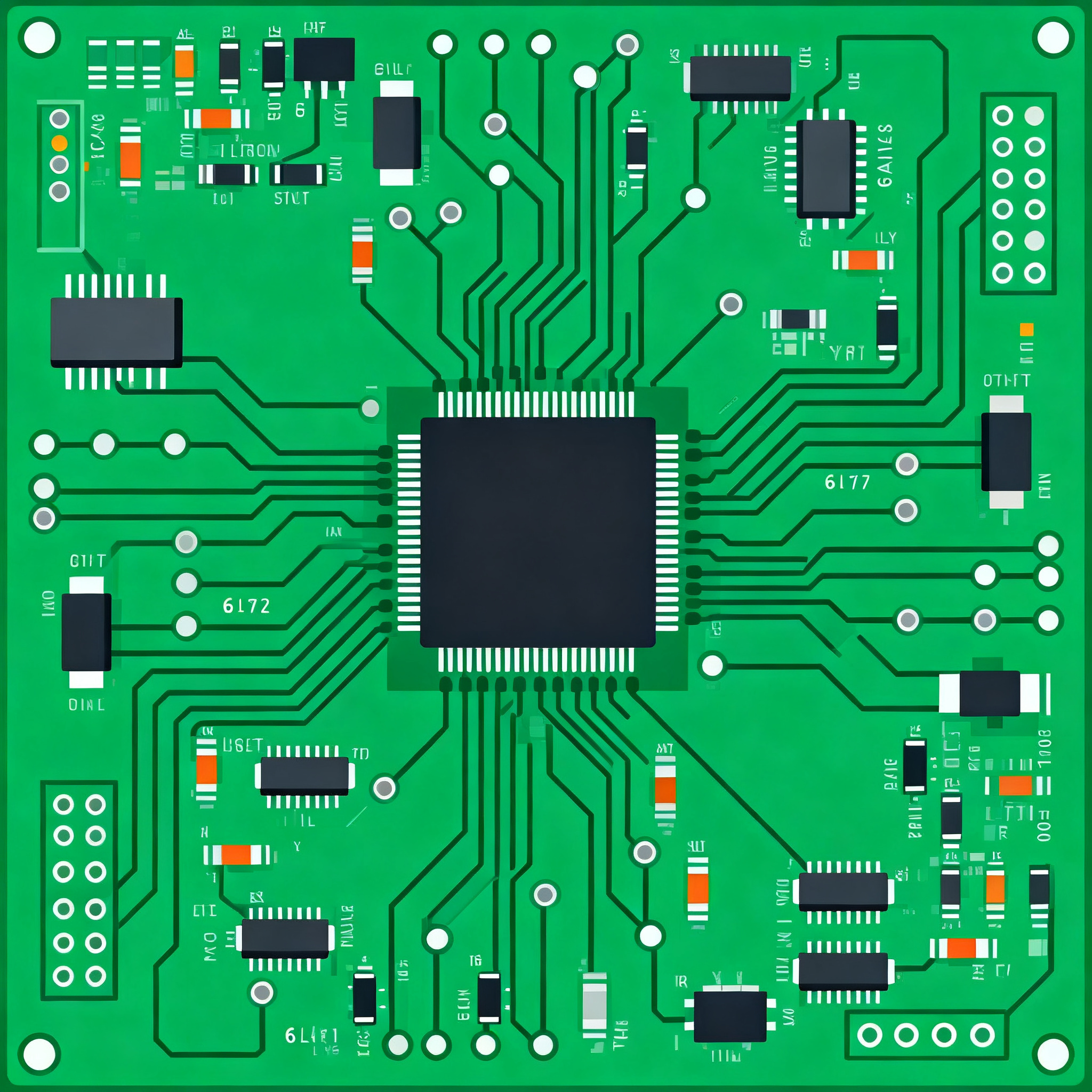
Detailed Specifications
When designing a 6-layer PCB, several specifications are crucial to consider. These include component values, layout dimensions, and material selection, all of which impact performance and cost. Precise calculations for resistance, capacitance, and inductance are essential for optimal circuit functionality. The following table outlines key design parameters and calculations necessary for effective PCB design.
| Parameter | Value | Formula/Calculation |
|---|---|---|
| Trace Width | 0.15 mm | Based on IPC-2221 standards |
| Dielectric Constant | 4.2 | Material dependent |
| Impedance | 50 Ohms | Z = √(L/C) |
| Capacitance | 2.2 nF | C = ε(A/d) |
| Inductance | 10 nH | L = (μN²A)/l |
| Board Thickness | 1.6 mm | Standard thickness |
| Via Diameter | 0.3 mm | Based on design rules |
| Copper Thickness | 35 μm | 1 oz copper |
| Power Supply Voltage | 3.3V | Standard logic level |
| Operating Temperature | -40°C to 85°C | Industrial standard |
Key Takeaways from the Specifications
The design parameters outlined in the table provide a foundation for creating efficient and cost-effective 6-layer PCB designs. Understanding the relationship between trace width, impedance, and material properties is crucial for optimizing signal integrity and minimizing losses. The specified component values ensure that the circuit can handle the required current and voltage levels, while the board thickness and via diameter are selected to meet industry standards. These specifications are critical for maintaining performance while reducing manufacturing costs, ensuring that the final product meets both technical and budgetary requirements.
| Parameter | Value | Analysis |
|---|---|---|
| Gain | 10 dB | High gain for signal amplification |
| Bandwidth | 2 GHz | Wide bandwidth for high-speed applications |
| Noise | 2 μV | Low noise for clear signals |
| Power Consumption | 500 mW | Efficient power usage |
| Thermal Dissipation | 0.8 W | Effective heat management |
| Signal Integrity | Excellent | Minimal signal loss |
| Reliability | High | Long-term performance assurance |
| Latency | 1 ns | Low latency for fast processing |
| Cross-Talk | Negligible | Reduced interference between signals |
| ESD Protection | Integrated | Prevents electrostatic damage |
Practical Implications
The performance analysis highlights the critical aspects of a 6-layer PCB design that influence its effectiveness in real-world applications. High gain and wide bandwidth are essential for applications requiring signal amplification and high-speed data transmission. Low noise and excellent signal integrity ensure clarity and reliability, while efficient power consumption and effective thermal dissipation contribute to the overall efficiency of the system. These parameters, combined with high reliability and integrated ESD protection, make the design suitable for a variety of demanding environments, ensuring that the PCB can perform optimally under different conditions.
| Configuration | Pros | Cons |
|---|---|---|
| Standard 6-Layer | Cost-effective, versatile | Limited to moderate complexity |
| High-Density Interconnect (HDI) | Compact, high performance | Higher cost, complex manufacturing |
| Embedded Components | Space-saving, improved reliability | Challenging repairs, higher initial cost |
| Flexible PCB | Lightweight, adaptable to shapes | More expensive, less durable |
| Rigid-Flex PCB | Durable, versatile | Complex design, higher cost |
| Metal Core PCB | Excellent heat dissipation | Heavier, more costly |
| Blind/Buried Vias | Space-efficient, improved performance | Complex design, higher cost |
Application Guidelines
The design trade-offs table provides insight into selecting the appropriate PCB configuration based on specific application requirements. Standard 6-layer PCBs offer a balance between cost and versatility, making them suitable for general applications. For high-performance needs, HDI and embedded components provide superior functionality but at a higher cost. Flexible and rigid-flex PCBs are ideal for applications requiring adaptability and durability, while metal core PCBs are best for high-heat environments. Understanding these trade-offs allows engineers to make informed decisions, optimizing design for performance and cost.
Design Considerations
Designing a cost-effective 6-layer PCB requires careful consideration of several factors, including material selection, component placement, and signal routing. The choice of materials impacts both performance and cost, with options like FR-4 providing a balance of affordability and reliability. Component placement should minimize trace lengths to reduce signal loss and interference, while strategic routing can enhance signal integrity. Employing design-for-manufacturability (DFM) practices ensures that the PCB can be produced efficiently, reducing waste and lowering costs. Additionally, utilizing simulation tools can help identify potential issues early in the design process, saving time and resources.
Step-by-Step Implementation
Creating an optimized 6-layer PCB design involves several critical steps:
- Define the project requirements, including performance, size, and budget constraints.
- Select appropriate materials and components based on the project’s specifications.
- Create a preliminary layout, focusing on efficient component placement and routing.
- Utilize simulation tools to test the design for signal integrity and thermal performance.
- Iterate the design based on simulation feedback, optimizing for cost and performance.
- Prepare detailed documentation, including schematics and bill of materials (BOM).
- Engage with manufacturing partners early to ensure design compatibility with fabrication processes.
- Conduct thorough testing of prototypes to validate design assumptions and performance.
Common Issues & Solutions
When developing a 6-layer PCB, several common issues may arise:
- Signal Integrity Problems: Address by optimizing trace widths and using proper grounding techniques.
- Thermal Management: Implement heat sinks or thermal vias to dissipate excess heat.
- Manufacturing Defects: Mitigate by adhering to IPC standards and performing regular inspections.
- Cost Overruns: Control by selecting cost-effective materials and components without compromising quality.
- Component Sourcing Delays: Avoid by establishing strong relationships with reliable suppliers and maintaining a buffer stock.
- Design Complexity: Simplify by focusing on essential features and minimizing unnecessary layers or components.
Applications & Use Cases
6-layer PCBs are utilized across various industries due to their versatility and performance. In telecommunications, they enable high-speed data processing and signal transmission. In the automotive sector, they are used in advanced driver assistance systems (ADAS) and infotainment systems. Consumer electronics, such as smartphones and tablets, benefit from their compact size and reliability. Medical devices utilize 6-layer PCBs for precision and durability, while industrial applications leverage their robustness for automation and control systems. Each application leverages the unique advantages of 6-layer designs to meet specific operational demands.
Selection & Sourcing Guide
Selecting and sourcing the right components for a 6-layer PCB design is crucial for performance and cost efficiency. Utilize online resources like IC Online to explore a wide range of components and materials. Consider factors such as lead time, cost, and supplier reliability when making sourcing decisions. Establishing partnerships with trusted suppliers can ensure timely delivery and quality assurance, reducing the risk of production delays and cost overruns.
FAQ
- What materials are best for 6-layer PCBs? FR-4 is commonly used for its balance of cost and performance, but high-frequency applications may require advanced materials like Rogers.
- How can I reduce costs in multilayer PCB designs? Optimize layout, use standard components, and choose cost-effective materials to minimize expenses.
- What is the typical lead time for manufacturing a 6-layer PCB? Lead times can vary, but quick-turn services like those offered by Nova PCBA can expedite production.
- How do I ensure signal integrity in a complex PCB design? Proper grounding, controlled impedance, and minimizing trace lengths are key strategies.
- What tools are available for PCB design and simulation? Software like Altium Designer, Eagle, and KiCad are popular choices for PCB design and simulation.
- How can I integrate thermal management in my PCB design? Use thermal vias, heat sinks, and appropriate copper weights to manage heat dissipation.
- What are the challenges of using HDI technology? While offering high performance, HDI technology can increase manufacturing complexity and cost.
- What is the importance of IPC standards in PCB design? IPC standards ensure quality, reliability, and manufacturability, reducing the risk of defects.
- How can I validate my PCB design before manufacturing? Use simulation and prototyping to test and validate design assumptions and performance.
- What is the role of a bill of materials (BOM) in PCB design? A BOM lists all components and materials, serving as a reference for sourcing and production.
Conclusion
Cost optimization in 6-layer PCB projects requires a strategic approach, balancing performance and budget constraints. By understanding circuit topology, performing detailed component calculations, and analyzing performance, designers can make informed decisions that reduce costs without sacrificing quality. Adhering to industry standards, employing advanced simulation tools, and leveraging reliable manufacturing partners are crucial steps in achieving successful, cost-effective PCB designs. Ultimately, these strategies enable engineers to deliver high-performance solutions that meet the demands of today's competitive electronics market.