Cost Breakdown: Analyzing Multilayer PCB Costs for Budget-Conscious Engineers
Cost Breakdown: Analyzing Multilayer PCB Costs for Budget-Conscious Engineers Introduction In the rapidly evolving electronics industry, the demand for compact, high-performance, and cost-effective so...
Introduction
In the rapidly evolving electronics industry, the demand for compact, high-performance, and cost-effective solutions is ever-growing. Multilayer PCBs are central to this demand, offering enhanced functionality and reduced footprint. However, understanding the cost implications of designing and manufacturing multilayer PCBs is crucial for engineers who need to balance performance with budget constraints. This article delves into the cost breakdown of multilayer PCBs, focusing on key design rules, stackup configurations, signal integrity, and manufacturing considerations.
Technical Overview
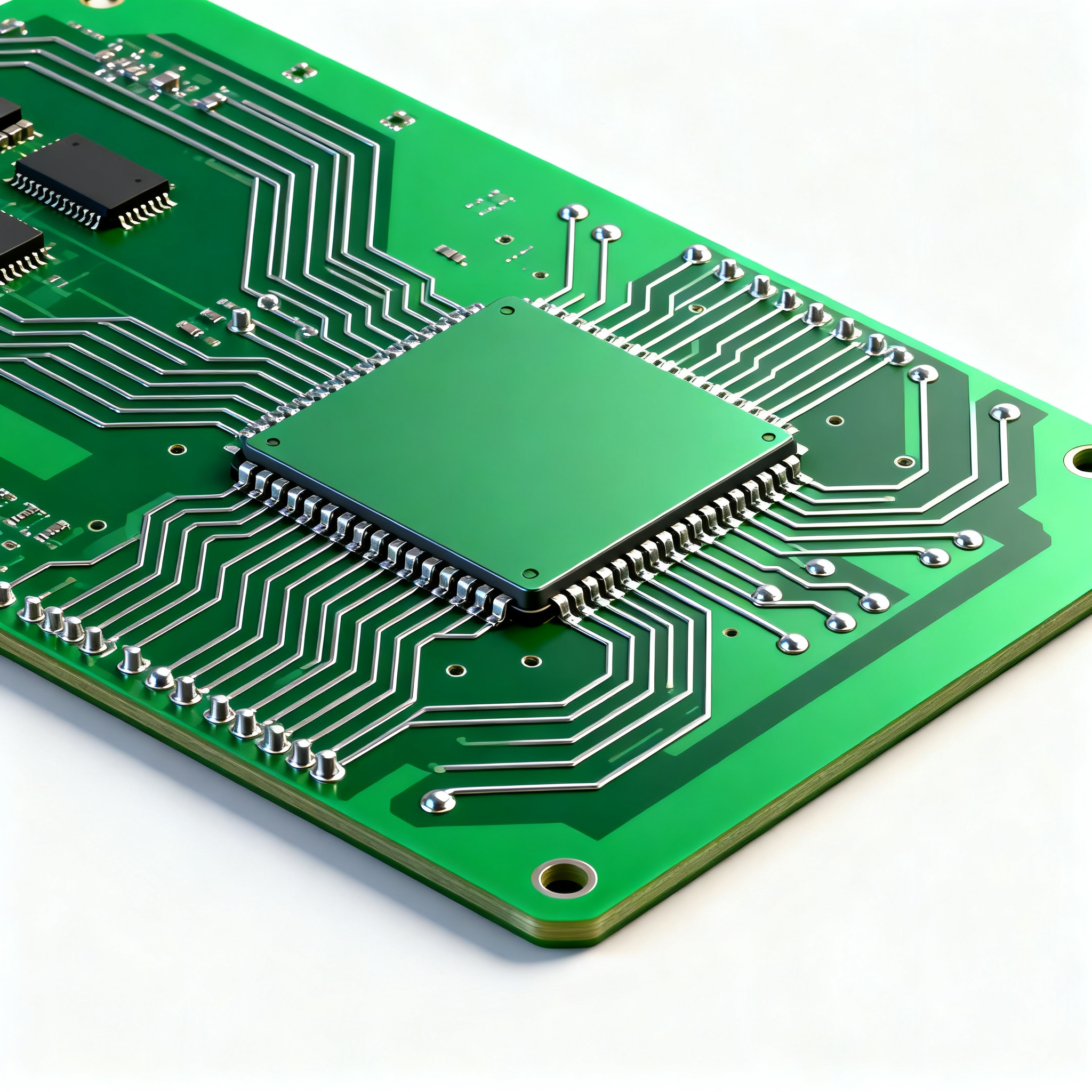
Multilayer PCBs consist of multiple layers of conductive and insulating materials laminated together. These layers allow for complex circuit designs, enabling higher component density and improved electrical performance. The architecture of a multilayer PCB is defined by factors such as the number of layers, the choice of materials, and the specific design rules applied. Core concepts like trace width, spacing, via sizes, and clearances are critical in ensuring signal integrity and reliability. Additionally, stackup design plays a pivotal role in mitigating electromagnetic interference (EMI) and maintaining signal quality.
Detailed Specifications
When designing a multilayer PCB, several specifications must be considered to ensure optimal performance and manufacturability. These include trace width, spacing, via sizes, and clearances. Adhering to these specifications is vital for maintaining signal integrity and ensuring the board can be manufactured efficiently and cost-effectively. Below is a detailed table outlining common PCB design rules.
| Design Rule | Minimum Value | Notes |
|---|---|---|
| Trace Width | 0.1 mm | Depends on current carrying capacity |
| Trace Spacing | 0.1 mm | Critical for preventing short circuits |
| Via Diameter | 0.3 mm | Includes annular ring |
| Via Hole Size | 0.2 mm | Drill tolerance is considered |
| Clearance from Edge | 0.5 mm | Prevent electrical shorts |
| Layer-to-Layer Spacing | 0.2 mm | Ensures insulation between layers |
| Pad Size | 0.5 mm | For component soldering |
| Minimum Annular Ring | 0.1 mm | Ensures reliable connections |
| Silkscreen to Pad Clearance | 0.15 mm | Avoids solder mask exposure |
| Minimum Solder Mask Dam | 0.1 mm | Prevents solder bridging |
Key Takeaways from the Specifications
The specifications outlined in the table above are essential for ensuring that a multilayer PCB design is both functional and manufacturable. Trace width and spacing are critical for maintaining signal integrity and preventing short circuits. Proper via sizing and clearance are necessary for reliable connections and avoiding potential electrical shorts. These design rules are guided by industry standards such as IPC-2221 and are crucial for achieving a balance between performance and cost-effectiveness.
| Layer Configuration | Number of Layers | Applications |
|---|---|---|
| 2-Layer | 2 | Simple designs, low-cost applications |
| 4-Layer | 4 | Improved signal integrity, reduced EMI |
| 6-Layer | 6 | High-speed digital applications |
| 8-Layer | 8 | Complex designs, RF applications |
| 10-Layer | 10 | Advanced computing, data processing |
| 12-Layer | 12 | High-density interconnect (HDI) designs |
| 14-Layer | 14 | Telecommunications, networking equipment |
Practical Implications
The choice of layer stackup is pivotal in determining the performance and cost of a PCB. A 2-layer stackup is suitable for low-cost, simple designs, while more complex applications may require 6-layer or 12-layer configurations to enhance signal integrity and reduce EMI. Each additional layer increases manufacturing complexity and cost, making it crucial to match the stackup with the specific application requirements. Engineers must consider the trade-offs between performance, complexity, and budget when selecting a stackup configuration.
| Material | Dielectric Constant (Dk) | Loss Tangent |
|---|---|---|
| FR-4 | 4.5 | 0.02 |
| Rogers 4350B | 3.66 | 0.0037 |
| Rogers 4003C | 3.55 | 0.0027 |
| Isola FR408HR | 3.7 | 0.008 |
| Nelco N4000-13 | 3.7 | 0.009 |
| Arlon 85N | 3.5 | 0.004 |
| Polyimide | 4.2 | 0.02 |
| PTFE | 2.1 | 0.001 |
| Megtron 6 | 3.6 | 0.004 |
| Panasonic R-5515 | 3.7 | 0.005 |
Application Guidelines
The material properties of a PCB significantly influence its performance and suitability for specific applications. FR-4 is a common choice due to its cost-effectiveness and adequate performance for many applications. However, for high-frequency applications, materials like Rogers 4350B or PTFE, with lower dielectric constants and loss tangents, are preferred to minimize signal loss. Engineers must select materials based on the specific electrical and thermal requirements of their application, balancing performance with cost.
Design Considerations
When designing a multilayer PCB, engineers must consider a range of factors to ensure optimal performance and manufacturability. Key considerations include:
- Adhering to industry standards such as IPC-2221 for design rules and IPC-4101 for material specifications.
- Ensuring adequate trace width and spacing to handle the required current levels and prevent crosstalk.
- Choosing an appropriate stackup configuration to balance performance with manufacturing costs.
- Selecting materials that meet the thermal and electrical requirements of the application.
- Incorporating design for manufacturability (DFM) principles to reduce production costs and improve yield.
By carefully considering these factors, engineers can design PCBs that meet performance requirements while staying within budget constraints.
Step-by-Step Implementation
- Define the Requirements: Start by clearly defining the performance, size, and cost requirements for your PCB.
- Select the Stackup: Choose the appropriate number of layers and materials based on your design's complexity and application.
- Design the Schematic: Create a detailed schematic that outlines the electrical connections and component placements.
- Layout the PCB: Use PCB design software to layout the traces, vias, and components, adhering to design rules.
- Perform Signal Integrity Analysis: Simulate the PCB to ensure signal integrity and minimize EMI.
- Review and Optimize: Review the design for manufacturability and cost optimization, making adjustments as needed.
- Prototype and Test: Fabricate a prototype of the PCB and perform thorough testing to validate the design.
- Finalize Production: Once testing is complete, finalize the design for mass production, ensuring all documentation is accurate.
Common Issues & Solutions
- Issue: Signal Integrity Problems
Solution: Optimize trace width and spacing, and use proper grounding techniques. - Issue: High EMI
Solution: Implement a well-planned layer stackup and use shielding techniques. - Issue: Manufacturing Defects
Solution: Adhere to DFM guidelines and perform thorough design reviews. - Issue: Thermal Management
Solution: Use appropriate materials with good thermal properties and design for adequate heat dissipation. - Issue: Cost Overruns
Solution: Balance performance with cost by selecting the right materials and simplifying the design where possible.
Applications & Use Cases
Multilayer PCBs are used in a variety of applications across different industries:
- Consumer Electronics: Smartphones, tablets, and laptops utilize multilayer PCBs for compact and high-performance designs.
- Telecommunications: Networking equipment and communication devices rely on multilayer PCBs for efficient signal processing.
- Automotive: Modern vehicles use multilayer PCBs in advanced driver assistance systems (ADAS) and infotainment systems.
- Aerospace: Avionics and satellite systems require robust multilayer PCBs for reliable performance in extreme environments.
Selection & Sourcing Guide
When selecting and sourcing materials for multilayer PCBs, engineers should consider factors such as material properties, supplier reliability, and cost. For a comprehensive list of components and suppliers, visit IC Online.
FAQ
- What is the typical cost of a multilayer PCB?
The cost varies depending on the number of layers, materials used, and manufacturing complexity. Generally, it ranges from $10 to $100 per unit for small to medium production runs. - How does the number of layers affect PCB cost?
More layers increase complexity and material use, leading to higher costs. Each additional layer adds approximately 20-30% to the base cost of a 2-layer PCB. - What are the benefits of using high-frequency materials?
High-frequency materials, such as Rogers, offer lower dielectric loss and better signal integrity for RF and microwave applications. - How can I reduce EMI in my PCB design?
Use proper grounding techniques, optimize layer stackup, and consider using shielding materials or components. - What design software is recommended for multilayer PCBs?
Popular options include Altium Designer, Eagle, and KiCad, each offering robust tools for multilayer design. - How do I ensure my PCB design is manufacturable?
Follow DFM guidelines, consult with your manufacturer early in the design process, and perform thorough design reviews. - What is the importance of the dielectric constant in PCB materials?
The dielectric constant affects signal speed and impedance; materials with lower constants are preferred for high-speed applications. - Can I use standard FR-4 for high-frequency applications?
While possible, FR-4 is not ideal due to higher loss tangent; consider using specialized materials like Rogers for better performance. - What are common via types in multilayer PCBs?
Common via types include through-hole, blind, and buried vias, each suited for different design needs. - How can I ensure signal integrity in a high-speed PCB design?
Focus on proper trace impedance control, minimize crosstalk, and ensure adequate power distribution.
Conclusion
Designing and manufacturing multilayer PCBs requires careful consideration of various factors, including design rules, stackup configurations, material properties, and cost implications. By understanding these elements, engineers can create efficient, high-performance PCBs that meet the demands of modern applications while staying within budget constraints. Leveraging industry standards and best practices is key to achieving successful outcomes in PCB design and manufacturing.