Common PCB Assembly Defects: Troubleshooting Tips for Reliable Production
Common PCB Assembly Defects: Troubleshooting Tips for Reliable Production table { border-collapse: collapse; width: 100%; margin: 20px 0; } th, td { border: 1px solid #000; padding: 8px; } thead { bac...
Introduction
In the fast-evolving world of electronics, the reliability of Printed Circuit Boards (PCBs) is paramount. With the increasing complexity of electronic devices, ensuring the quality and functionality of PCBs is more critical than ever. Common PCB assembly defects can lead to malfunction, impacting the overall performance of electronic products. Understanding these defects and implementing effective troubleshooting strategies is essential for reliable PCB production. This article delves into the intricacies of PCB design rules, stackup design, signal integrity, and manufacturing considerations, providing a comprehensive guide to avoiding common pitfalls.
Technical Overview
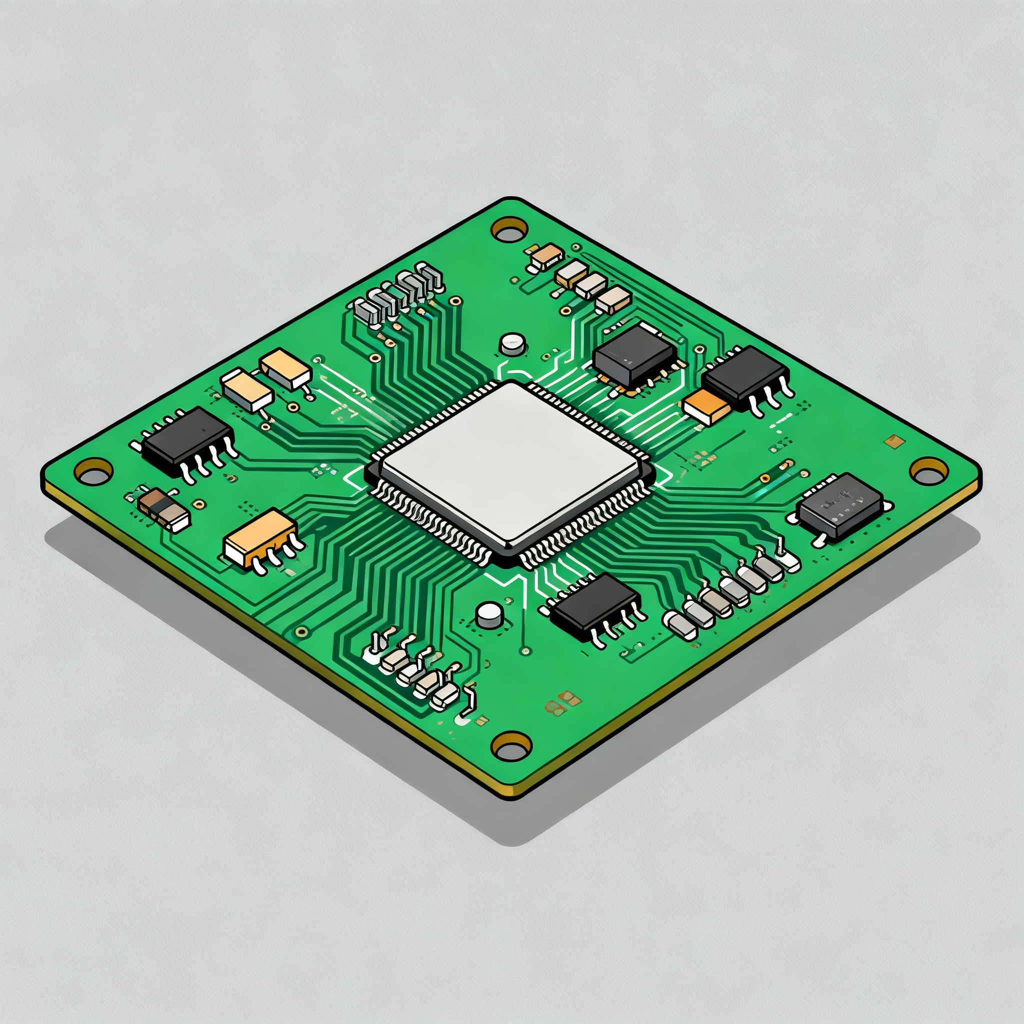
PCBs serve as the backbone of electronic devices, providing the mechanical support and electrical connections needed for components to function. The design and manufacturing process involves several key elements: PCB layout rules, layer stackup, signal integrity, and manufacturing considerations. Each aspect plays a crucial role in ensuring the board's performance and reliability. PCB layout rules dictate the physical arrangement of traces, vias, and components, while stackup design influences the board's electromagnetic compatibility and thermal performance. Signal integrity involves maintaining the quality of electrical signals across the board, and manufacturing considerations address the practical aspects of production, including material selection and assembly techniques. Together, these elements form the foundation of a successful PCB design and manufacturing process.
Detailed Specifications
Understanding the specifications of PCB design is crucial for optimizing performance and reliability. Key specifications include trace width, spacing, via sizes, and clearances, which directly affect the board's functionality and manufacturability. These parameters must adhere to industry standards and be carefully calculated to ensure signal integrity and prevent issues such as crosstalk and interference.
| Design Parameter | Standard Value | Importance |
|---|---|---|
| Trace Width | 0.15 mm | Ensures adequate current carrying capacity |
| Trace Spacing | 0.15 mm | Prevents electrical shorts |
| Via Size | 0.3 mm | Facilitates layer transitions |
| Clearance | 0.2 mm | Avoids crosstalk and interference |
| Pad Size | 0.6 mm | Ensures component stability |
| Annular Ring | 0.1 mm | Ensures via reliability |
| Drill Hole Size | 0.25 mm | Accommodates component leads |
| Aspect Ratio | 10:1 | Ensures manufacturability |
| Solder Mask Clearance | 0.05 mm | Prevents solder bridging |
| Silkscreen Clearance | 0.1 mm | Ensures legibility |
| Minimum Feature Size | 0.1 mm | Supports high-density designs |
| Layer Count | Up to 12 | Accommodates complex circuits |
Key Takeaways from the Specifications
Understanding the data in the above table is crucial for successful PCB design. The trace width and spacing are fundamental for maintaining signal integrity and preventing shorts. Via sizes and clearances ensure reliable layer transitions and minimize crosstalk. Adhering to these specifications helps in achieving a balance between performance and manufacturability, leading to more reliable and efficient PCBs. These parameters should be carefully calculated and verified against industry standards such as the IPC-2221 to ensure compliance and functionality.
| Layer Configuration | Typical Use | Advantages |
|---|---|---|
| 2-Layer | Simple circuits | Cost-effective |
| 4-Layer | Moderate complexity | Improved signal integrity |
| 6-Layer | Complex circuits | Better power distribution |
| 8-Layer | High-density designs | Enhanced EMI shielding |
| 10-Layer | Advanced applications | Superior signal integrity |
| 12-Layer | High-speed applications | Optimal for high-performance |
| 16-Layer | Cutting-edge technology | Maximum routing capability |
Practical Implications
The choice of layer stackup configuration significantly impacts the performance and cost of a PCB. For example, a 2-layer board is suitable for simple applications, offering a cost-effective solution. However, as complexity increases, a 4-layer or 6-layer configuration may be necessary to ensure adequate signal integrity and power distribution. Advanced applications may require up to 16 layers to accommodate high-speed signals and provide maximum routing capability. Understanding these configurations helps designers select the appropriate stackup to meet specific performance requirements while managing costs effectively.
| Material | Dielectric Constant (Dk) | Loss Tangent |
|---|---|---|
| FR-4 | 4.5 | 0.02 |
| Rogers 4350B | 3.48 | 0.0037 |
| Rogers 4003C | 3.55 | 0.0027 |
| Isola FR408HR | 3.68 | 0.009 |
| Nelco N4000-13 | 3.7 | 0.008 |
| Megtron 6 | 3.6 | 0.003 |
| Arlon 85N | 3.5 | 0.004 |
| Panasonic R-1755V | 3.9 | 0.005 |
| DuPont Pyralux | 3.2 | 0.0040 |
| Taconic RF-35 | 3.5 | 0.0018 |
Application Guidelines
Material selection is a critical aspect of PCB design, influencing both electrical performance and cost. FR-4 is a standard material offering a balance between performance and cost, suitable for a wide range of applications. For high-frequency applications, materials like Rogers 4350B and Taconic RF-35 provide lower loss tangents, enhancing signal integrity. Understanding the dielectric constant and loss tangent of materials helps designers make informed decisions, ensuring the selected material meets the specific requirements of their application, whether it be high-speed, high-frequency, or cost-sensitive designs.
Design Considerations
When designing PCBs, several practical guidelines must be followed to avoid common assembly defects and ensure reliable production. Firstly, it's essential to adhere to design rules for trace width, spacing, and clearance to prevent electrical shorts and crosstalk. Proper layer stackup design is crucial for managing electromagnetic interference and maintaining signal integrity. The choice of materials should align with the application's electrical requirements and budget constraints. Additionally, it's vital to incorporate test points to facilitate troubleshooting and quality inspection. Employing design for manufacturability (DFM) principles can significantly improve production efficiency and reduce costs. By considering these factors early in the design process, engineers can minimize potential issues and enhance the overall reliability of the PCB.
Step-by-Step Implementation
Implementing a robust PCB design involves several key steps:
- Define Requirements: Clearly outline the electrical, mechanical, and environmental requirements of the PCB based on the end application.
- Schematic Design: Create a detailed schematic diagram to define the electrical connections and component relationships.
- Component Selection: Choose components that meet the design specifications, considering factors such as availability, cost, and performance.
- PCB Layout: Design the PCB layout, adhering to design rules for trace width, spacing, and via sizes to ensure manufacturability and reliability.
- Layer Stackup Design: Select an appropriate layer stackup configuration to meet signal integrity and power distribution requirements.
- Material Selection: Choose PCB materials that provide the necessary electrical properties while balancing cost considerations.
- Design Validation: Use simulation tools to verify the design's electrical performance and identify potential issues before fabrication.
- Prototype Fabrication: Manufacture a prototype to test the design's functionality and identify any assembly defects.
- Testing and Inspection: Perform thorough testing and inspection to verify the PCB's performance against the design specifications.
- Production and Quality Control: Once validated, proceed to full-scale production, implementing quality control measures to ensure consistency and reliability.
Common Issues & Solutions
Despite careful design, PCBs can encounter various assembly defects. Here are some common issues and their solutions:
- Insufficient Solder Joint: Ensure proper solder paste application and reflow profile to achieve consistent solder joints.
- Solder Bridging: Use appropriate solder mask clearance and inspect stencil design to prevent bridging between pads.
- Component Misalignment: Verify pick-and-place machine calibration and use fiducial markers for accurate component placement.
- Delamination: Select materials with suitable thermal properties and optimize reflow profiles to prevent layer separation.
- Insufficient Through-Hole Fill: Ensure proper via design and soldering techniques to achieve complete through-hole fill.
- Electromagnetic Interference (EMI): Implement proper grounding and shielding techniques to minimize EMI issues.
Applications & Use Cases
PCBs are integral to a wide range of applications, from consumer electronics to industrial and automotive systems. In consumer electronics, PCBs are used in smartphones, tablets, and wearable devices, where compact size and high performance are crucial. In industrial applications, PCBs must withstand harsh environments and provide reliable performance in machinery and control systems. Automotive PCBs require high reliability and thermal management to operate in the challenging conditions of vehicles. Understanding the specific requirements of each application helps in designing PCBs that meet the necessary performance and reliability standards.
Selection & Sourcing Guide
When selecting and sourcing components for PCB production, it's important to consider factors such as availability, cost, and performance. Online resources like IC Online provide a comprehensive database of electronic components, enabling designers to find the right parts for their projects. It's essential to work with reputable suppliers to ensure component quality and availability, minimizing the risk of delays in production.
FAQ
- What are the most common PCB assembly defects? Common defects include insufficient solder joints, solder bridging, and component misalignment.
- How can I improve signal integrity in my PCB design? Use proper trace width and spacing, select appropriate materials, and design an optimal layer stackup to enhance signal integrity.
- What materials are best for high-frequency applications? Materials like Rogers 4350B and Taconic RF-35, with low loss tangents, are ideal for high-frequency applications.
- How do I choose the right layer stackup for my PCB? Consider the application's complexity, signal integrity requirements, and cost constraints when selecting a layer stackup configuration.
- What is the role of the IPC standards in PCB design? IPC standards provide guidelines for PCB design, assembly, and quality inspection, ensuring compliance and reliability.
- How can I prevent solder bridging during assembly? Use proper solder mask clearance and stencil design, and verify the reflow profile to prevent bridging.
- What is the importance of design for manufacturability (DFM)? DFM principles help optimize the design for efficient production, reducing costs and minimizing defects.
- How do I ensure component availability for my PCB design? Work with reputable suppliers, use online resources like IC Online, and consider alternate parts to ensure availability.
- What are the benefits of using a multi-layer PCB? Multi-layer PCBs provide better signal integrity, power distribution, and EMI shielding, supporting complex and high-speed applications.
- How do I test and validate my PCB design? Use simulation tools and prototype fabrication to test the design's electrical performance and identify potential issues before full-scale production.
Conclusion
Ensuring reliable PCB production involves understanding and addressing common assembly defects, adhering to design rules, and selecting the right materials and configurations. By following industry standards and implementing best practices, designers can create PCBs that meet performance and reliability requirements across various applications. This comprehensive guide provides the knowledge and tools necessary to troubleshoot common issues and optimize PCB design and manufacturing processes.