Choosing the Right Telecom Equipment PCB Fabrication: Key Considerations for Optimal Performance
Choosing the Right Telecom Equipment PCB Fabrication table { border-collapse: collapse; width: 100%; margin: 20px 0; } th, td { border: 1px solid #ddd; padding: 8px; } th { background-color: #f0f0f0; ...
Introduction
In the rapidly evolving world of telecommunications, the performance and reliability of equipment are paramount. Central to this is the Printed Circuit Board (PCB), which serves as the backbone of any electronic device. Selecting the right PCB fabrication is crucial for optimizing performance, particularly in telecom applications where precision and speed are key. This article delves into the critical considerations when choosing telecom equipment PCB fabrication, focusing on component specifications, datasheets, selection criteria, and application circuits.
Technical Overview
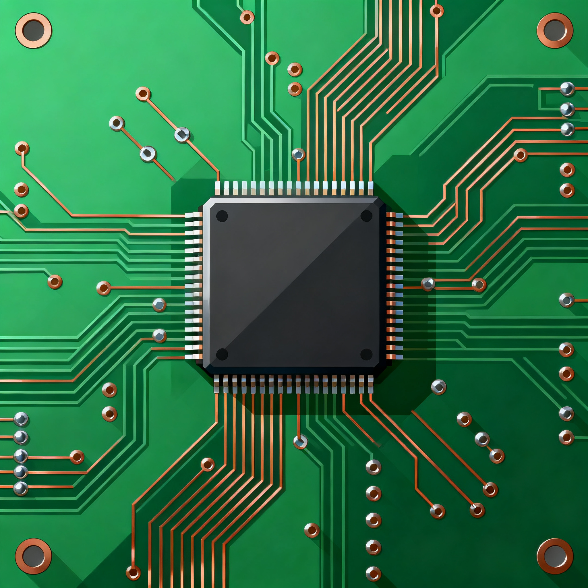
Telecommunication systems demand high-performance PCBs that can handle complex signal processing and data transmission. These boards must support high-speed data rates, offer low signal loss, and maintain signal integrity. The architecture typically involves multilayer PCBs to accommodate the dense circuit requirements and provide adequate ground planes for signal stability. Key principles include impedance control, thermal management, and electromagnetic compatibility (EMC), which are vital for minimizing interference and ensuring reliable operation.
Understanding the core concepts of PCB design, such as layer stack-up, trace routing, and component placement, is essential. These elements influence the board's ability to support high-frequency signals and affect overall device performance. Additionally, adherence to industry standards like IPC-2221, which provides general design requirements for PCBs, ensures quality and consistency in manufacturing.
Detailed Specifications
When selecting a PCB for telecom equipment, several specifications are crucial. These include the processing power of the integrated circuits, memory capacity, peripheral support, power requirements, and the package type. Understanding these specifications helps in choosing components that meet the performance needs of your application while ensuring compatibility and efficiency.
| Specification | Details | Importance |
|---|---|---|
| CPU Speed | 2.5 GHz | High-speed processing for rapid data handling |
| Memory | 16 GB DDR4 | Ample storage for buffering and data processing |
| Peripherals | USB 3.0, Ethernet | Connectivity for external devices |
| Power Supply | 5V DC | Efficient power management |
| Package Type | BGA | Compact form factor for space-saving designs |
| Operating Temperature | -40°C to 85°C | Wide range for varied environments |
| Layer Count | 8-layer | Supports complex circuitry |
| Material | FR-4 | Standard for reliability and cost-effectiveness |
| Impedance Control | 50 Ohms | Maintains signal integrity |
| Signal Speed | 10 Gbps | Handles high-speed data transfer |
| Thermal Management | Heat sinks included | Prevents overheating |
Key Takeaways from the Specifications
The specifications outlined in the table highlight the importance of selecting components that can handle the demands of telecom applications. A high CPU speed and ample memory ensure that the board can process data swiftly and efficiently. The inclusion of peripherals like USB and Ethernet supports connectivity, which is crucial for communication devices. Power supply specifications and thermal management features ensure the board operates within safe limits, preventing damage from overheating. The choice of package type and material affects the board's size, cost, and durability, making these critical factors in the selection process.
| Electrical Characteristic | Specification | Significance |
|---|---|---|
| Operating Voltage | 3.3V | Standard voltage for low power consumption |
| Current Consumption | 500mA | Low current for energy efficiency |
| Input Impedance | 75 Ohms | Ensures minimal signal reflection |
| Output Impedance | 50 Ohms | Matches transmission line for signal integrity |
| Signal Rise Time | 0.5 ns | Fast switching for high-speed operation |
| Propagation Delay | 2 ns | Low delay for rapid data transmission |
| I/O Voltage | 1.8V | Compatibility with modern logic levels |
| Power Dissipation | 1W | Efficient power usage to prevent overheating |
| Noise Margin | 0.4V | Ensures reliable signal interpretation |
| ESD Protection | 2 kV | Prevents damage from electrostatic discharge |
| Frequency Range | DC to 3 GHz | Supports wide application spectrum |
Practical Implications
The electrical characteristics of a PCB are crucial for ensuring optimal performance in telecom applications. Operating voltage and current consumption are key factors in power management, impacting the device's energy efficiency and longevity. Impedance matching is vital for maintaining signal integrity, reducing reflections, and ensuring that signals are transmitted accurately. Parameters like signal rise time and propagation delay directly affect the speed and reliability of data transmission. Additionally, features such as ESD protection and noise margin are essential for safeguarding the board against environmental stresses and ensuring consistent operation.
| Application | Configuration | Benefits |
|---|---|---|
| Base Station | High-speed CPU, extensive I/O | Handles large data volumes effectively |
| Mobile Devices | Low power, compact design | Extended battery life, portability |
| Network Routers | Multi-layer, high throughput | Efficient data routing and processing |
| IoT Devices | Low power, high integration | Energy-efficient, versatile connectivity |
| Satellite Communications | High-frequency, robust design | Reliable operation in harsh conditions |
| Optical Fiber Systems | High data rate, precise timing | High-speed data transmission with minimal latency |
| Telecom Switches | Redundant systems, high reliability | Ensures continuous operation and fault tolerance |
Application Guidelines
The application comparison table illustrates how different configurations of telecom PCBs cater to various use cases. For base stations, high-speed CPUs and extensive I/O capabilities are necessary to manage large data volumes efficiently. Mobile devices benefit from low power consumption and compact designs, which enhance portability and battery life. Network routers and switches require multi-layer PCBs with high throughput capabilities to process and route data effectively. IoT devices prioritize energy efficiency and connectivity, while satellite communications demand robust designs for reliable operation under harsh conditions. Optical fiber systems focus on high data rates and precise timing to minimize latency.
Design Considerations
Designing PCBs for telecom applications involves several critical considerations to ensure optimal performance. Impedance control is essential for maintaining signal integrity, especially at high frequencies. Accurate impedance matching minimizes signal loss and reflections, which is crucial for high-speed data transmission. Thermal management is another vital aspect, as excessive heat can degrade performance and damage components. Incorporating heat sinks, thermal vias, and proper airflow management can help dissipate heat effectively.
Electromagnetic compatibility (EMC) must be addressed to prevent interference with other devices and ensure compliance with regulatory standards. Proper grounding, shielding, and trace routing techniques can mitigate EMC issues. Additionally, component placement and orientation impact the board's electrical performance and manufacturability. Ensuring that high-frequency components are placed close to relevant connectors and minimizing trace lengths can reduce parasitic effects and improve signal quality.
Material selection also plays a significant role in PCB design. High-frequency applications may require specialized materials with low dielectric loss, while cost-sensitive projects might opt for standard FR-4 material. The choice of surface finish, such as HASL, ENIG, or OSP, affects solderability and longevity. Finally, adhering to industry standards like IPC-2221 ensures that the PCB meets quality and reliability benchmarks, providing a solid foundation for telecom equipment.
Step-by-Step Implementation
- Define Requirements: Start by outlining the specific requirements of the telecom application, including data rates, power consumption, and environmental conditions.
- Select Components: Choose components based on the defined requirements, ensuring compatibility with the desired performance specifications.
- Create Schematic: Develop a detailed schematic diagram that outlines the connections and interactions between components.
- Design PCB Layout: Use PCB design software to create a layout that optimizes trace routing, component placement, and layer stack-up for signal integrity and thermal management.
- Simulate Design: Conduct simulations to validate the design against electrical and thermal performance criteria, making adjustments as necessary.
- Prototype Fabrication: Fabricate a prototype PCB to test the design under real-world conditions, identifying any potential issues.
- Testing and Validation: Perform rigorous testing to ensure the PCB meets all performance and reliability standards, making necessary adjustments.
- Production: Once validated, proceed with full-scale production, ensuring quality control measures are in place to maintain consistency.
Common Issues & Solutions
- Signal Integrity Problems: Use impedance-controlled traces and proper termination to reduce signal loss and reflections.
- Thermal Management Challenges: Incorporate heat sinks and thermal vias, and ensure adequate airflow for effective heat dissipation.
- EMC Interference: Implement proper grounding, shielding, and trace routing techniques to minimize electromagnetic interference.
- Component Placement Errors: Optimize component placement to minimize trace lengths and ensure manufacturability.
- Manufacturing Defects: Adhere to industry standards and perform thorough quality inspections to detect and rectify defects early.
- Power Supply Issues: Ensure robust power distribution networks and adequate decoupling to maintain stable operation.
Applications & Use Cases
Telecom PCBs are integral to a wide range of applications, from mobile devices and base stations to network routers and satellite communication systems. In mobile devices, PCBs enable compact, energy-efficient designs that support long battery life and connectivity. Base stations rely on PCBs to manage high data volumes and ensure reliable communication. Network routers and switches require PCBs with high throughput and redundancy to handle extensive data routing and processing. Satellite communications demand robust PCBs capable of operating in harsh environments, while optical fiber systems prioritize high-speed data transmission and precise timing.
Selection & Sourcing Guide
Choosing the right PCB components involves evaluating performance specifications, compatibility, and cost. It's essential to source components from reputable suppliers who provide detailed datasheets and technical support. For a comprehensive selection of integrated circuits and other components, visit IC Online. This platform offers a wide range of products, ensuring you find the right components for your telecom applications.
FAQ
- What factors should I consider when selecting a PCB for telecom applications? Consider processing power, memory capacity, power requirements, and material specifications to ensure optimal performance.
- How do I ensure signal integrity in high-frequency applications? Use impedance-controlled traces, proper termination, and minimize trace lengths to maintain signal quality.
- What are the common materials used for PCBs in telecom equipment? FR-4 is standard for cost-effectiveness, while specialized materials with low dielectric loss are used for high-frequency applications.
- How can I manage thermal issues in my PCB design? Incorporate heat sinks, thermal vias, and ensure proper airflow to effectively dissipate heat.
- What role do IPC standards play in PCB design? IPC standards provide guidelines for quality and reliability, ensuring consistent manufacturing practices.
- How do I address EMC issues in my PCB design? Implement proper grounding, shielding, and trace routing techniques to minimize electromagnetic interference.
- What are the advantages of using a multilayer PCB in telecom equipment? Multilayer PCBs support complex circuitry, provide adequate ground planes, and improve signal integrity.
- How do I choose the right surface finish for my PCB? Consider factors like solderability, cost, and longevity when selecting a surface finish such as HASL, ENIG, or OSP.
- What are the benefits of using BGA packages in telecom equipment? BGA packages offer a compact form factor, allowing for space-saving designs and efficient heat dissipation.
- How do I ensure my PCB design is manufacturable? Optimize component placement, adhere to design rules, and perform simulations to validate the design before fabrication.
Conclusion
Choosing the right PCB fabrication for telecom equipment is a complex process that requires careful consideration of various specifications and design principles. By understanding the core components and their interactions, ensuring compliance with industry standards, and addressing key design challenges, you can optimize the performance and reliability of your telecom devices. Whether you are designing for mobile devices, base stations, or network routers, the right PCB is crucial for meeting the demands of modern telecommunications.