Avoiding Pitfalls: Top Strategies for PCB Design Error Prevention
Avoiding Pitfalls: Top Strategies for PCB Design Error Prevention table { border-collapse: collapse; width: 100%; margin: 20px 0; } th, td { border: 1px solid #ddd; padding: 8px; } th { background-col...
Introduction
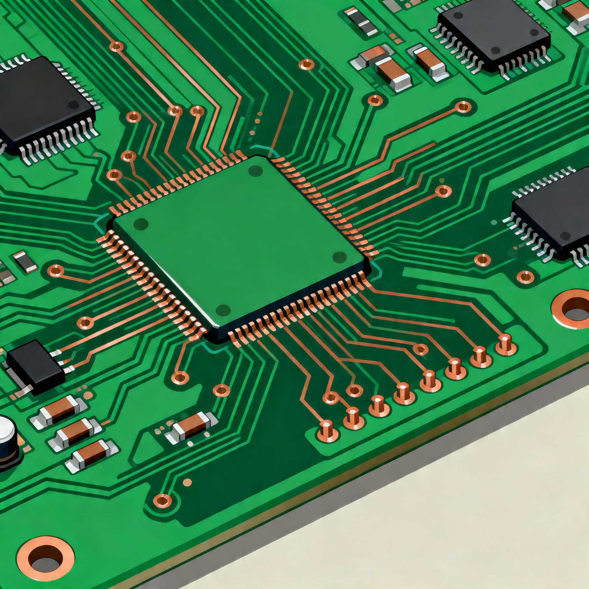
In the fast-paced world of electronics, the design of printed circuit boards (PCBs) is a critical task that requires precision and strategic planning. PCB design affects the performance, reliability, and manufacturability of electronic devices. With increasing complexity in electronic circuits, avoiding design errors is paramount to ensure product success and avoid costly reworks. This article delves into strategies for preventing PCB design errors, focusing on circuit topology, component calculations, performance analysis, and design trade-offs.
Technical Overview
PCB design encompasses several core concepts, including circuit topology, which defines the arrangement of components and their interconnections. A well-thought-out topology ensures signal integrity and efficient power distribution. Component calculations are vital to ensure that components operate within their specified limits. Performance analysis evaluates parameters such as gain, bandwidth, noise, and power consumption to ensure the PCB meets its operational requirements. Design trade-offs often involve balancing competing requirements, such as cost versus performance or size versus functionality.
Detailed Specifications
Specifications are the backbone of PCB design, dictating the choices of components, layout, and overall design strategy. Key specifications include component values, which must be calculated accurately to ensure the circuit functions as intended. Calculations involve using formulas to determine the correct resistor, capacitor, and inductor values, among others. Understanding these specifications is crucial for designing a PCB that meets performance criteria and reliability standards.
| Component | Value | Calculation Formula |
|---|---|---|
| Resistor | 1kΩ | V = IR |
| Capacitor | 10µF | Q = CV |
| Inductor | 100µH | V = L(di/dt) |
| Diode | 1N4001 | Vf = 0.7V (Si) |
| Transistor | BC547 | Ic = βIb |
| Op-Amp | LM741 | Vout = A(V+ - V-) |
| LED | 5mm, 20mA | If = (Vcc - Vf)/R |
| Crystal Oscillator | 16MHz | f = 1/(2π√LC) |
| Voltage Regulator | LM7805 | Vout = Vin - Vdrop |
| Thermistor | 10kΩ | R = R0 * exp(B(1/T - 1/T0)) |
Key Takeaways from the Specifications
The table above outlines crucial component values and their associated calculation formulas, which are foundational for any PCB design. Each component's value and its formula ensure the circuit operates under the desired electrical conditions. For instance, the resistor value determines current flow, while the capacitor affects the circuit's timing characteristics. By accurately calculating these values, designers can avoid common pitfalls such as overheating, inefficiencies, or component failure, thereby ensuring optimal circuit performance.
| Parameter | Value | Impact |
|---|---|---|
| Gain | 20dB | Amplifies signal |
| Bandwidth | 100MHz | Determines frequency range |
| Noise | 5µV | Affects signal clarity |
| Power Consumption | 500mW | Impacts battery life |
| Signal-to-Noise Ratio | 60dB | Signal quality |
| Response Time | 10ns | Affects speed |
| Efficiency | 85% | Energy utilization |
| Temperature Range | -40°C to 85°C | Operating environment |
| Impedance | 50Ω | Signal matching |
| Latency | 1ms | Delay in signal processing |
Practical Implications
The performance analysis table highlights key parameters that define the operational characteristics of a PCB. Gain, bandwidth, and noise are critical for ensuring signal fidelity and clarity. Power consumption is a crucial consideration for battery-operated devices, impacting their longevity. Analyzing these parameters allows designers to tailor the PCB to meet specific application needs, ensuring that the device performs efficiently under varying conditions. Understanding these impacts aids in making informed design choices, balancing performance with practical constraints.
| Configuration | Pros | Cons |
|---|---|---|
| Single Layer | Low cost, simple design | Limited routing |
| Double Layer | Increased routing options | Higher cost |
| Multilayer | Compact size, high density | Complex manufacturing |
| Rigid | Durable, reliable | Less flexible |
| Flexible | Versatile, lightweight | More expensive |
| Rigid-Flex | Best of both worlds | Complex design |
| High-Frequency | Supports RF applications | Special materials needed |
| Power PCB | Handles high current | Thermal management needed |
Application Guidelines
The design trade-offs table provides insights into different PCB configurations and their respective advantages and disadvantages. For instance, single-layer PCBs are cost-effective but limited in routing options, making them suitable for simple applications. On the other hand, multilayer PCBs offer high density and compact size, ideal for complex and space-constrained designs. Understanding these trade-offs helps designers choose the right configuration based on application requirements, budget constraints, and manufacturing capabilities.
Design Considerations
When embarking on PCB design, several practical considerations must be addressed to avoid common pitfalls. First, adhering to industry standards such as IPC guidelines ensures compliance with best practices and quality benchmarks. Proper component placement and routing are crucial for minimizing electromagnetic interference and ensuring thermal management. It's essential to perform a thorough design review, involving simulation and prototyping, to validate functionality before full-scale production. Additionally, considering manufacturability from the outset can prevent costly redesigns and ensure smooth production processes.
Step-by-Step Implementation
Implementing a successful PCB design involves several detailed steps. First, define the design requirements, including electrical specifications, size constraints, and environmental conditions. Next, create a schematic diagram, selecting suitable components and ensuring correct connections. Perform simulations to validate the circuit's performance against the specifications. Once the schematic is verified, proceed with the PCB layout, focusing on optimal component placement and routing. Conduct a design rule check (DRC) to identify and rectify any layout issues. Manufacture a prototype and conduct thorough testing to ensure the PCB meets all performance criteria. Finally, prepare technical documentation and production files for mass manufacturing.
Common Issues & Solutions
PCB design often encounters several challenges. One common issue is signal integrity problems due to improper routing or impedance mismatches, which can be mitigated by following good design practices and using simulation tools. Thermal management is another critical aspect, as excessive heat can lead to component failure; using thermal vias and heat sinks can alleviate this. Component selection errors can be avoided by cross-referencing datasheets and using verified libraries. Manufacturing defects such as solder bridges can be minimized by adhering to design for manufacturability (DFM) guidelines. Lastly, power distribution issues can be addressed by ensuring adequate power plane design and decoupling capacitors.
Applications & Use Cases
PCBs are integral to a wide range of applications, from consumer electronics like smartphones and laptops to industrial equipment and automotive systems. In the medical field, PCBs are used in devices such as MRI machines and patient monitors. In telecommunications, they form the backbone of networking equipment and mobile devices. The versatility of PCBs makes them suitable for custom applications, where specific design requirements must be met to achieve desired functionalities.
Selection & Sourcing Guide
Choosing the right components and materials is crucial for a successful PCB design. Utilize resources like IC Online to source reliable components. Consider factors such as lead time, cost, and supplier reputation. Ensure that components meet the required specifications and have been tested for compatibility with the intended application. Collaborating with reputable manufacturers, such as those listed in [PCBWay](https://www.pcbway.com/) and [Nova PCBA](https://www.novapcba.com/), can facilitate efficient production and assembly processes.
FAQ
1. What are the critical steps in PCB design?
The critical steps include defining requirements, schematic design, simulation, layout design, prototyping, testing, and documentation.
2. How do I ensure signal integrity in my PCB design?
Ensure proper routing, impedance matching, and use of ground planes and decoupling capacitors to maintain signal integrity.
3. What are some common PCB design errors?
Common errors include incorrect component values, poor layout, insufficient thermal management, and inadequate power distribution.
4. How can I prevent overheating in my PCB?
Use thermal management techniques such as heat sinks, thermal vias, and adequate spacing between heat-generating components.
5. What tools are recommended for PCB design?
Popular tools include Altium Designer, Eagle, KiCad, and OrCAD, each offering various features for different design needs.
6. How do I choose the right PCB configuration?
Consider factors such as complexity, cost, size, and application requirements when selecting a PCB configuration.
7. What is the importance of design rule checks?
Design rule checks help identify and correct errors in the layout, ensuring compliance with manufacturing capabilities and standards.
8. How can I improve the reliability of my PCB?
Follow industry standards, use quality components, perform thorough testing, and ensure robust design practices to enhance reliability.
Conclusion
Effective PCB design is a meticulous process that demands attention to detail and adherence to best practices. By understanding the intricacies of circuit topology, component calculations, and performance analysis, designers can avoid common pitfalls and create reliable, high-performance PCBs. Leveraging design trade-offs and practical guidelines ensures that the final product meets the intended application requirements. With a strategic approach and the right resources, PCB designers can confidently navigate the complexities of modern electronics design.