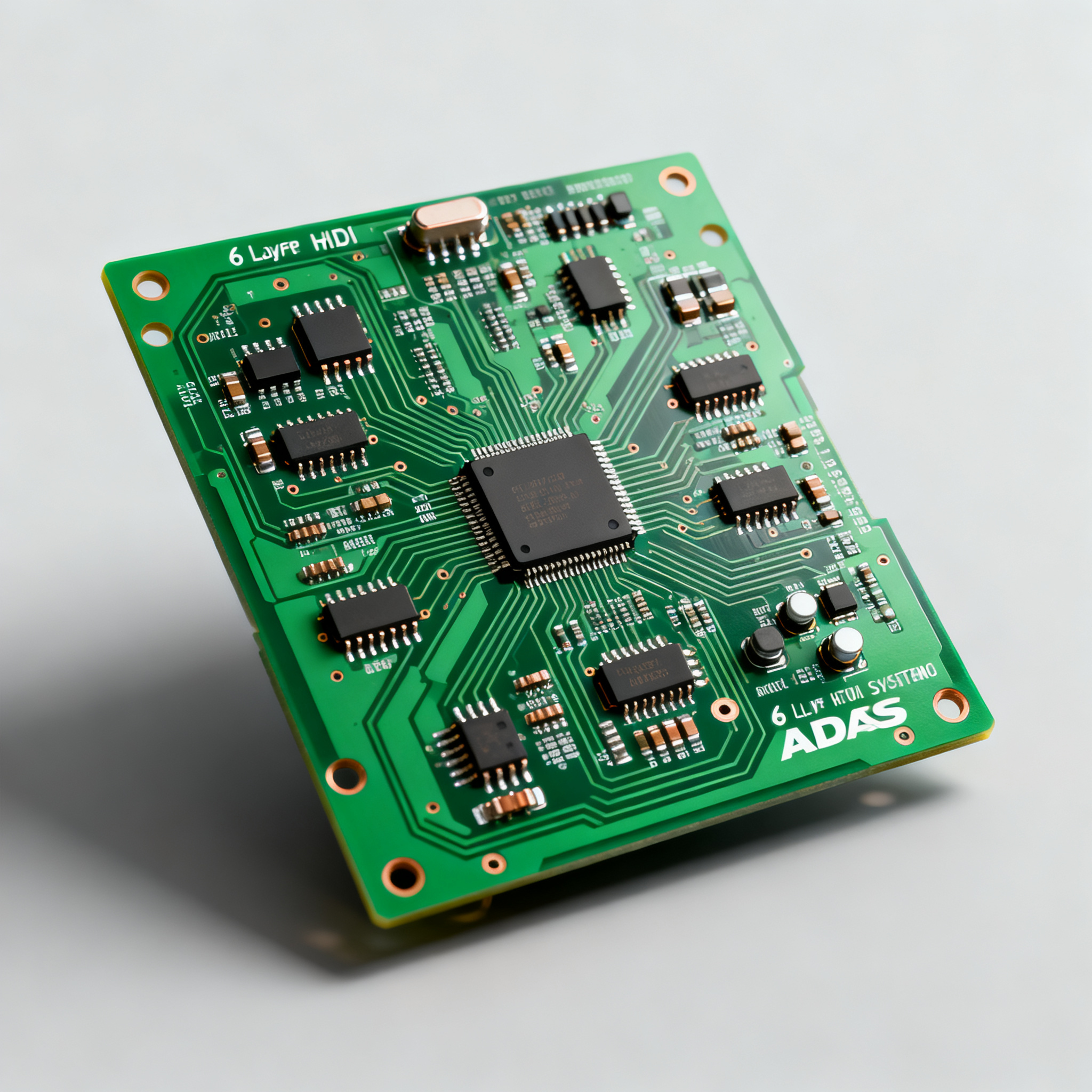
Automotive PCB Assembly Selection Guide: Comparing IATF 16949-Certified 6-Layer HDI Suppliers for ADAS Systems
When a $0.50 Component Choice Risks a $10M ADAS Recall: The Case for IATF 16949-Certified Assembly An ADAS control module failure at highway speed is not a warranty claim — it is a potential fatality....
When a $0.50 Component Choice Risks a $10M ADAS Recall: The Case for IATF 16949-Certified Assembly
An ADAS control module failure at highway speed is not a warranty claim — it is a potential fatality. Automotive engineers understand this calculus intimately, yet procurement teams still face pressure to shave pennies from BOM costs. The math collapses under scrutiny. As industry analysts at PCBSync quantify: a $0.50 cost saving per component evaporates the moment it triggers a $10 million recall. That figure does not account for regulatory fines, brand erosion, or litigation exposure.
IATF 16949 exists precisely to close this gap between procurement arithmetic and field reliability. Unlike ISO 9001 — which PC Tech Magazine correctly identifies as the baseline requirement, not an automotive-specific credential — IATF 16949 mandates defect prevention, not defect detection. BestPCBs articulates the distinction clearly: "No quality standard can guarantee absolute zero defects — but IATF 16949 is designed to make defects rare, predictable, and preventable." The operative word is predictable. A non-certified shop may deliver 98% yield on a 6-layer HDI ADAS board; the two failures per hundred are statistical noise — until they correlate with via barrel cracks in thermal cycling, and your entire production batch becomes suspect.
For ADAS systems — where a single PCB hosts radar signal processing, camera fusion, and decision-path logic on a 6-layer HDI stack — the supplier selection decision is fundamentally a risk-management exercise. The certification badge on the wall matters less than the process controls behind it. NextPCB's automotive sourcing guide reinforces this by emphasizing supply chain resilience requirements: a certified supplier must demonstrate not just process capability, but continuity-of-supply planning, duplicate tooling strategies, and documented escalation paths for out-of-specification events.
Key Takeaway: IATF 16949 certification is not a quality guarantee — it is a predictability guarantee. For ADAS systems where intermittent failures are unacceptable, predictability is the only currency that matters.
What Makes a 6-Layer HDI Stack-Up Survive Under the Hood: IPC-6012E Class 3 and Thermal Stress Testing
ADAS electronics live in a hostile environment. Under-hood temperatures swing from −40°C cold-soak to +125°C sustained operation within a single drive cycle. Vibration profiles reach 10G on engine-mounted modules. Humidity condenses, evaporates, and condenses again. A 6-layer HDI PCB carrying high-speed differential pairs for radar and camera data cannot afford a single microvia crack — because that crack becomes a signal integrity failure, and that failure becomes a braking decision made on corrupted sensor data.
The physics of reliability in this environment centers on three failure mechanisms. First, microvia fatigue: the coefficient of thermal expansion (CTE) mismatch between copper plating (≈17 ppm/°C) and the surrounding dielectric drives cyclic stress at the via barrel-to-pad interface. Second, conductive anodic filament (CAF) growth: moisture absorption in the laminate, combined with voltage bias between adjacent plated structures, causes copper ions to migrate along glass-fiber interfaces, creating resistive shorts. Third, interconnect stress due to HDI layer transitions: stacked or staggered microvias in a 6-layer build concentrate mechanical stress at the layer-1-to-layer-2 and layer-5-to-layer-6 transitions.
PCBMaster explains that IATF 16949 enhances ISO 9001 precisely in these areas: documented product safety management processes and mechanical testing for resistance to thermal stress and physical deformation become mandatory, not optional. PCBOnline reinforces this with a deep dive into the manufacturing processes that differentiate automotive-grade HDI production — particularly controlled-depth laser drilling, plasma desmear, and electrolytic copper plating with tight thickness uniformity.
The table below captures the measurable differences between a consumer-grade 6-layer HDI board and one built to IPC-6012E Class 3 with IATF 16949 process controls. These are not theoretical values — they are the acceptance criteria your supplier's quality engineer should be able to produce test data against.
| Reliability Parameter | Consumer-Grade HDI (IPC Class 2) | Automotive-Grade HDI (IPC Class 3, IATF 16949) | Failure Consequence for ADAS |
|---|---|---|---|
| Microvia plating thickness (min.) | 15–18 µm | 20–25 µm (IPC-6012DA) | Thinner plating reduces cycles to barrel fatigue crack initiation |
| Thermal cycling endurance | 100 cycles (−40°C to +125°C) | 1,000 cycles min. per IPC-6012E Class 3 | Intermittent open circuits after 6–12 months of field operation |
| CAF resistance testing | Not required | 500+ hours at 85°C/85% RH with bias voltage | Dendritic shorts between adjacent signal traces on ADAS sensor inputs |
| Copper elongation (plated through-hole) | ≥12% | ≥18% (IPC-6012DA) | Higher ductility absorbs CTE mismatch stress without cracking |
| Dielectric spacing (inner-layer) | 0.10 mm typical | 0.15 mm minimum for HV isolation | Breakdown on radar power supply rails under humidity soak |
| Via-in-pad fill material | Non-conductive epoxy (optional) | Conductive copper fill or capped epoxy, verified by X-ray | Solder voiding under BGA packages on ADAS processor ICs |
| Laminate CTE (Z-axis, pre-Tg) | 50–70 ppm/°C | ≤45 ppm/°C (low-CTE FR-4 or polyimide) | Lower Z-axis expansion reduces PTH barrel stress |
| Lot-level traceability | Date-code only | Full serialization: laminate lot, plating cell, AOI records | Inability to contain a latent defect to a specific production window |
The gap between 100 and 1,000 thermal cycles is not a marginal improvement — it represents the difference between surviving one year of daily driving and surviving the 15-year design life of a vehicle. NextPCB's automotive-grade PCB guide highlights that IPC-6012E Class 3 also imposes stricter annular ring requirements and plating void criteria for microvias, which directly affect the long-term reliability of via-in-pad structures under BGA packages on ADAS processor boards.
Tip: When requesting qualification data from a supplier, ask specifically for thermal cycling test reports that run to failure, not just to the 1,000-cycle acceptance threshold. The Weibull characteristic life (η) of the microvia population tells you more about field reliability than a pass/fail report.
IATF 16949-Certified 6-Layer HDI Suppliers: Beyond the Certificate — Comparing DFM, Via-in-Pad, and Regional Resilience
An IATF 16949 certificate hanging in the lobby tells you the supplier passed an audit. It does not tell you whether they passed it with a robust, deeply embedded quality culture or with a last-minute document scramble. For ADAS-grade 6-layer HDI boards, the certificate is the starting line, not the finish line.
PCBMaster describes the specific enhancements IATF 16949 brings over ISO 9001: documented product safety management processes, mandatory failure mode and effects analysis (FMEA) on every process step, and statistical process control (SPC) with defined reaction plans for out-of-control conditions. The depth to which these requirements are implemented varies significantly between certified suppliers. One shop may treat FMEA as a paperwork exercise; another uses it to drive real-time process adjustments.
PCBSync adds a critical dimension: regional manufacturing options reduce logistics risk and lead times. A 6-layer HDI ADAS board shipped across three borders introduces transit-induced thermal shock, customs delays, and communication latency when quality issues arise. RapidDirect provides a capacity benchmark: top-tier certified suppliers operate at 45,000 m²/month PCB and 150,000 pcs/month PCBA capacity with multiple SMT lines — scale that translates to scheduling flexibility when your ADAS program ramps from prototype to production.
NextPCB's IATF 16949 certification serves as a useful reference point: a supplier that achieved certification by demonstrating in-house laser drilling capability, via-in-pad process control, and documented IPC Class 3 yield data. When evaluating suppliers, use this as your benchmark — not the certificate alone, but the specific capabilities that certification required the supplier to validate.
The comparison framework below helps you evaluate suppliers on the dimensions that matter for ADAS HDI production, not just the presence of a certificate.
| Evaluation Criterion | Minimum Acceptable (Certified Supplier) | Preferred (High-Maturity IATF 16949 Supplier) | How to Verify |
|---|---|---|---|
| Laser drilling capability | Outsourced or shared laser; single wavelength (CO₂ only) | In-house UV laser for blind microvias ≤100 µm; dual-wavelength capability | Request equipment list with serial numbers; confirm during virtual audit |
| Via-in-pad process control | Epoxy fill with cap plating; visual inspection only | Copper-filled vias with X-ray verification of void content ≤5%; cross-section micrographs per lot | Demand cross-section images from 3 consecutive production lots |
| IPC Class 3 yield (6-layer HDI) | 92–95% first-pass yield | ≥97% first-pass yield with documented Pareto analysis of defect modes | Request 12-month rolling yield data, not a single "representative" month |
| Regional manufacturing footprint | Single site; 3+ weeks ocean freight to end customer | Multiple certified sites or nearshore option; ≤5-day air freight or local trucking | Map physical locations against your assembly plant; verify duplicate tooling |
| Prototype turnaround (6-layer HDI, traceable) | 10–14 working days | 5–7 working days with full lot traceability and same inspection gates as production | Place a paid trial order; verify lot-level serialization in the shipment |
| FMEA maturity | Generic process FMEA; reviewed annually | Design-specific FMEA updated per NPI; linked to SPC control limits and reaction plans | Request the FMEA for your specific stack-up; look for RPN values and mitigation actions |
| Product safety documentation | Certificate of conformance only | Full PPAP Level 3 submission including dimensional results, material certs, and process capability studies | Specify PPAP requirements in your RFQ; evaluate the completeness of the response |
A supplier that scores in the "Preferred" column across most criteria is not just certified — they have operationalized IATF 16949 into daily process discipline. The difference manifests in the defect rate: BestPCBs notes that certified suppliers deliver defect rates "an order of magnitude lower than non-certified shops." For an ADAS production run of 50,000 units, that is the difference between 50 field failures and 500.
Sourcing Traps That Compromise ADAS Reliability: How to Audit a 6-Layer HDI Supplier's Process, Not Just Their Paperwork
The most dangerous supplier is not the one without a certificate — it is the one with a certificate and a decaying process. IATF 16949 requires continuous improvement, but the audit cycle is annual. Between audits, process drift can erode the very controls the certificate represents.
BestPCBs is explicit on this point: IATF 16949 does not guarantee zero defects. It guarantees a framework for making defects rare, predictable, and preventable. The framework works only when the supplier executes it. Your job as the buyer is to verify execution, not just documentation.
Here are the most common sourcing traps and how to avoid them:
- The Certificate Trap: Assuming IATF 16949 certification alone ensures ADAS-grade reliability. What to do instead: Demand process-specific evidence — cross-section micrographs of microvias, thermal cycling data to failure, and CAF resistance test reports for your stack-up, not a generic qualification coupon.
- The Component Substitution Trap: Allowing the assembler to substitute non-AEC-Q qualified components to meet cost targets or availability constraints. PCBSync warns: "Even a $0.50 cost saving per component isn't worth a potential $10 million recall. Always specify AEC-Q100/Q200 qualified components for automotive applications, and verify your component supplier maintains IATF 16949 certification." The PCB and the components on it must both meet automotive-grade requirements — a certified board with commercial-grade ICs is a recall waiting to happen.
- The Traceability Gap: Accepting batch-level traceability when lot-level serialization is required. If a latent defect appears in field returns 18 months after production, you need to isolate the affected population to a specific laminate lot, plating cell, and reflow profile — not a 30-day production window. PCBMaster emphasizes that product safety management processes under IATF 16949 require traceability to enable effective containment.
- The In-House Illusion: Believing that in-house laser drilling or via fill means the process is controlled. What to do instead: Verify that the process is under statistical control — ask for control charts (X-bar and R) for microvia diameter, plating thickness, and via fill void content over the last 30 production lots. A process that is in-house but out of control is worse than a well-managed outsourced process.
- The Fast-Turn Shortcut: Using a different supplier or process for prototypes than for production. The prototype boards that pass qualification must be representative of production — same laminate, same plating chemistry, same inspection gates. NextPCB's automotive sourcing guide includes this in its quality audit checklist: verify that prototype and production lines use the same certified processes.
The table below provides a practical audit framework — questions to ask and evidence to demand — organized by the phase of supplier evaluation.
| Audit Phase | What to Request | Red Flag | Acceptable Response |
|---|---|---|---|
| Pre-qualification | Cross-section micrographs of microvias (blind vias, layer 1–2 and 5–6) | "We don't have cross-sections for this specific stack-up" | Provides images from 3 lots showing plating uniformity ≥20 µm, no barrel cracks, no separation at the capture pad |
| Pre-qualification | Thermal cycling data (1,000 cycles, −40°C to +125°C) with resistance change <10% | Data stops at 500 cycles; resistance change exceeds 10% before 1,000 cycles | Full Weibull analysis showing characteristic life (η) exceeding 1,500 cycles for the microvia population |
| Process audit | SPC control charts for laser drill diameter (last 30 lots) | No SPC data; Cpk <1.33; out-of-control points without documented corrective actions | Cpk ≥1.67; stable process mean; documented reaction plans for any out-of-control condition |
| Process audit | Desmear process control log (permanganate concentration, temperature, dwell time) | Manual logging only; no automated chemical monitoring | Automated titration and replenishment; data logged every 4 hours; traceable to each production panel |
| Component sourcing | AEC-Q100/Q200 qualification certificates for all active and passive components on the BOM | Mixed commercial and automotive-grade components; certificates more than 2 years old without renewal | 100% AEC-Q qualified components; certificates current; supplier maintains IATF 16949 certification |
| Production sign-off | PPAP Level 3 submission including dimensional report, material certs, and process capability (Cpk) for critical features | Offers PPAP Level 1 (warrant only); Cpk values below 1.33 for microvia diameter or plating thickness | Complete PPAP package; all critical characteristics at Cpk ≥1.67; documented approval from the supplier's quality representative |
Tip: The most revealing question you can ask during a supplier audit is not "Do you have this certificate?" but "Show me your last three internal non-conformance reports and the corrective actions taken." A supplier that openly shares their failures — and demonstrates systematic root-cause analysis and corrective action — is demonstrating the continuous improvement culture that IATF 16949 demands. A supplier that claims they have no non-conformances is either not looking hard enough or not telling the truth.
6-Layer HDI ADAS PCB Assembly: Questions a Senior Engineer Asks Before Signing Off
The following questions represent the final gate before supplier selection. They are the questions a senior ADAS hardware engineer or quality manager asks when the stakes include functional safety at highway speeds.
Q: Does IATF 16949 certification guarantee zero defects in 6-layer HDI ADAS boards?
No standard can guarantee zero defects, and any supplier claiming otherwise should be disqualified. IATF 16949 is a risk-management framework that makes defects rare, predictable, and preventable through mandatory failure mode analysis (FMEA), statistical process control (SPC), and continuous improvement requirements. BestPCBs articulates this clearly: the standard is designed to make defects predictable rather than reactive. Expect defect rates an order of magnitude lower than non-certified shops — typically in the range of 50–200 defects per million opportunities (DPMO) for certified suppliers versus 1,000–5,000+ DPMO for non-certified. However, always verify in-process inspection data: automated optical inspection (AOI) first-pass yield, electrical test fallout by defect category, and post-thermal-cycling continuity test results for your specific stack-up. The certificate tells you the supplier has a quality system; the data tells you whether it is working.
Q: What via-in-pad reliability data should I request for a 6-layer HDI ADAS design?
Request three specific deliverables. First, cross-section micrographs of microvias after 1,000 thermal cycles (−40°C to +125°C, 15-minute dwell, per IPC-6012E Class 3) showing the via barrel, capture pad interface, and surrounding dielectric with no cracks, separation, or plating voids. Second, CAF resistance test reports: 500+ hours at 85°C/85% relative humidity with DC bias voltage applied between adjacent via structures, demonstrating insulation resistance above 100 MΩ throughout the test. Third, plating thickness measurements for both the via barrel wall (target: 20–25 µm minimum) and the capture pad (target: 25–30 µm) using a calibrated metallographic microscope. PCBMaster notes that mechanical testing for thermal stress resistance is a mandatory element of IATF 16949 compliance for automotive PCBs. Reputable suppliers will provide this data as part of their Production Part Approval Process (PPAP) submission, typically at Level 3.
Q: How can I audit a supplier's Class 3 microvia process without an on-site visit?
A remote audit is feasible and effective if structured correctly. Request a virtual process walk-through using a live video feed — not a pre-recorded tour — focusing on three areas: laser drilling (verify UV laser capability for blind vias ≤100 µm diameter; confirm pulse energy and repetition rate are controlled and logged per panel), desmear and electroless copper control (verify automated chemical monitoring with real-time concentration data; confirm permanganate desmear process parameters are traceable to each production lot), and automated optical inspection records (request AOI defect maps and false-call rates for the last 10 HDI production lots). Combine this with third-party audit reports from your certifying body, historical yield data for similar 6-layer HDI builds, and — critically — a trial run of a representative test coupon containing microvias, via-in-pad structures, and impedance-controlled traces that matches your intended stack-up. NextPCB's supplier audit checklist provides a structured framework for evaluating these criteria remotely.
Q: What is the minimum lead time for a 6-layer HDI prototype run with IATF 16949 traceability?
Expect 7–10 working days for a fully traceable prototype run of a 6-layer HDI board. This timeline includes laser drilling (1 day), electroless copper and panel plating (1–2 days), pattern plating and etching (1–2 days), lamination and via fill (1–2 days), solder mask and surface finish (1 day), electrical test and AOI (1 day), and final inspection with documentation package assembly (1 day). Some certified suppliers, such as those benchmarked by RapidDirect, offer 12-hour express prototyping for simpler HDI stacks, but verify that the fast-turn process does not bypass lot-level traceability or inspection gates. A 12-hour turn that skips CAF coupon testing or uses a different plating chemistry than production is a false economy — the prototype data will not be representative of production reliability. Insist that the same certified process, same laminate lot control, and same inspection criteria apply to prototypes as to production volumes.
Q: Should I prioritize regional assembly to avoid logistics disruptions for ADAS production?
Yes. Regional sourcing reduces two distinct risks. First, transit-induced thermal shock: a 6-layer HDI board shipped via ocean freight from Asia to North America or Europe experiences 3–4 weeks of uncontrolled temperature and humidity cycling, which can initiate microvia fatigue before the board is even assembled. Second, lead-time volatility: port congestion, customs clearance delays, and geopolitical disruptions can extend lead times unpredictably. PCBSync recommends evaluating regional manufacturing options specifically to reduce logistics risk. When evaluating suppliers, look for those with multiple manufacturing sites or nearshore options — for example, a supplier with IATF 16949-certified facilities in both Asia and Mexico or Eastern Europe can offer regional flexibility. Ensure they maintain duplicate tooling and certified processes across locations so that a production transfer does not require re-qualification. The ideal configuration is a supplier that can deliver prototype volumes from a regional facility within 5 working days and scale to production volumes with the same certified process.
At NovaPCBA, we understand that ADAS PCB assembly is not a commodity purchase — it is a safety-critical supply chain decision. Our automotive assembly services are built on the same principles outlined in this guide: IATF 16949-aligned process controls, full lot-level traceability, and a commitment to providing the verification data engineers need to sign off with confidence. Whether you are qualifying a new 6-layer HDI design or auditing an existing supply chain, the questions above form the core of a rigorous supplier evaluation.
References & Further Reading
- IATF 16949 Certified PCB Supplier — BestPCBs — Defect prevention philosophy and practical implications of IATF 16949 certification for PCB manufacturing.