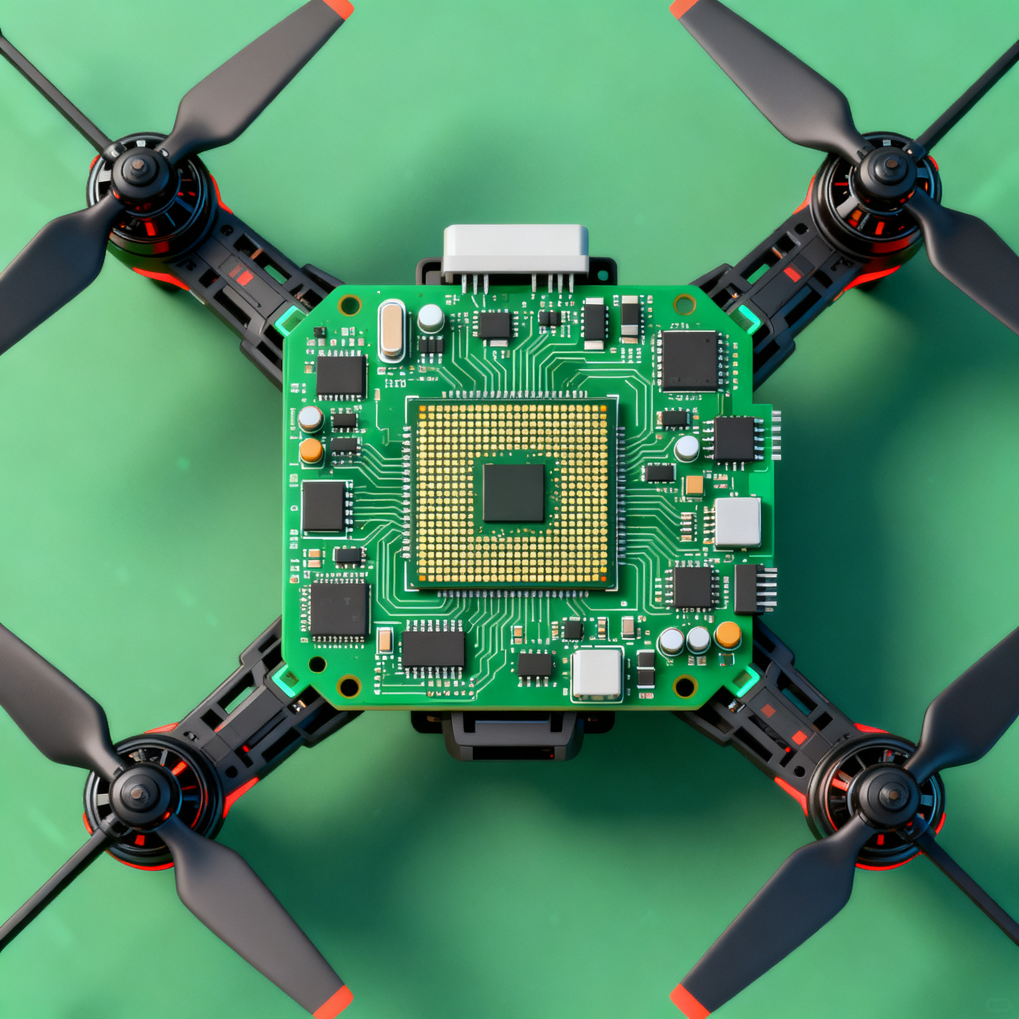
Aerial Photography Drone PCBA Cost Optimization: How Mixed-Signal BGA Assembly Reduces Per-Unit Spend
Aerial Photography Drone PCBA Cost Optimization: How Mixed-Signal BGA Assembly Reduces Per-Unit Spend Camera drone manufacturers face relentless pressure to shrink flight controller boards, cut weight...
Aerial Photography Drone PCBA Cost Optimization: How Mixed-Signal BGA Assembly Reduces Per-Unit Spend
Camera drone manufacturers face relentless pressure to shrink flight controller boards, cut weight, and lower bill-of-materials cost while preserving the signal integrity that delivers jitter-free 4K video and stable GPS/IMU fusion. The mixed-signal ball grid array (BGA) has emerged as the most direct path to achieving all three goals simultaneously. By integrating analog sensor front-ends, high-speed digital processing, and power management into a single compact package, a well-executed BGA design can slash per-unit PCBA spend by 20–35% compared to equivalent discrete or QFN-based layouts — without sacrificing RF performance or thermal headroom. This article walks you through the economics, design rules, and assembly trade-offs that make mixed-signal BGA the cost-optimization lever of choice for aerial photography drone electronics.
Why Mixed-Signal BGA Packages Are Reshaping Aerial Drone PCBA Economics
Consumer and prosumer camera drones have moved well beyond simple gyro-stabilized flight. Today’s platforms pack multi-axis gimbal controllers, obstacle-avoidance sensor arrays, 4K/60fps image signal processors, and dual-band Wi-Fi/Bluetooth connectivity onto a single mainboard. The traditional approach — spreading these functions across discrete op-amps, ADCs, MCUs, and PMICs in QFN or TSSOP packages — consumes excessive board area, forces higher layer counts, and multiplies the number of solder joints that can fail in the field.
A mixed-signal BGA flips that equation. By co-locating sensitive analog blocks (MEMS microphone interfaces, ambient light sensors, barometric pressure sensor conditioning) with a Cortex-M7 or similar processor core and multiple LDO/SMPS regulators, one package replaces 15–30 discrete components. The immediate effect is a smaller PCB footprint, which cascades into savings on laminate material, layer count, and enclosure size. For a mid-range aerial photography drone shipping 20,000 units annually, the move from a 6-layer QFN-based flight controller to a 4-layer BGA design can trim total PCBA cost by several dollars per board — enough to fund a better camera module or longer battery life.
This shift is well documented in industry guides to drone PCB optimization (elepcb.com), which emphasize that component integration is the single largest lever for reducing weight and assembly complexity. Meanwhile, manufacturers specializing in industrial-grade PCBA for aerial platforms (richpcba.com) report that mixed-signal BGA designs consistently yield higher first-pass yields in production because fewer placements mean fewer opportunities for tombstoning, billboarding, or cold joints. For the purchasing manager, that translates into predictable per-unit cost and shorter lead times.
How Mixed-Signal BGA Assembly Cuts Per-Board Cost Without Sacrificing Signal Integrity
The cost savings from a mixed-signal BGA don’t come from the package price alone — in fact, the BGA component itself may carry a modest premium over the sum of discrete parts. The real leverage lies in the PCB fabrication and assembly process. Fewer components mean fewer pick-and-place cycles, fewer solder paste deposits, and a smaller board outline that fits more units per panel. Critically, the reduced I/O breakout complexity often lets you drop from a 6-layer stackup to 4 layers, which can cut bare board cost by 25–40% depending on material and surface finish.
Signal integrity actually improves in many cases. With the analog front-end and ADC sitting micrometers from the processor die inside the BGA substrate, the sensitive nodes that would otherwise traverse inches of PCB trace are contained within a controlled-impedance package. This shortens the loop area for noise pickup and reduces the need for guard traces or additional ground planes. The result is cleaner sensor data — essential for the IMU and barometer inputs that stabilize a camera drone in gusty conditions.
The table below quantifies the typical design shift when moving from a QFN-based discrete flight controller to a mixed-signal BGA implementation. The values are drawn from real-world 4-layer and 6-layer designs for a mid-tier aerial photography drone with GPS, 3-axis gimbal control, and 1080p video downlink.
| Parameter | 6-Layer QFN Discrete Design | 4-Layer Mixed-Signal BGA Design | Cost Impact |
|---|---|---|---|
| Board outline | 45 × 45 mm | 35 × 35 mm | ~40% area reduction; more boards per panel |
| Layer count | 6 (signal-GND-signal-PWR-GND-signal) | 4 (signal-GND-PWR-signal) | 25–35% lower bare PCB cost |
| Total component count | 210 placements | 95 placements | Fewer reels, shorter pick-and-place time |
| Via count (total) | ~480 | ~260 | Reduced drill time, fewer via-in-pad requirements |
| Typical assembly yield (first pass) | 94–96% | 97–99% | Lower rework labor and scrap |
| Analog signal path length (IMU to ADC) | 35–50 mm | <5 mm (on-package) | Improved noise immunity, simpler layout |
| RF shielding requirement | Multiple discrete cans over LNA, PA, transceiver | Single compartment shield over BGA + passives | Fewer shield clips, faster assembly |
| Relative PCBA cost index (10k units/year) | 1.0 (baseline) | 0.65–0.75 | 25–35% total cost reduction |
These numbers align with the component integration challenges described in comprehensive drone PCB build guides (fs-pcba.com), which note that every eliminated connector, passive, or secondary IC reduces both the direct material cost and the hidden cost of inspection and rework. The key is to ensure that the BGA you select has a pinout optimized for easy breakout on four layers — something we’ll address in the design rules section.
BGA vs. QFN vs. LGA for Drone Flight Controllers: When Smaller Packages Pay Off
Not every drone flight controller benefits from a BGA. For low-complexity boards — a simple brushed-motor toy drone or a fixed-wing stabilizer with only a few sensors — QFN and LGA packages remain cost-effective and easier to prototype. But once you add a camera serial interface (CSI), multiple SPI sensor buses, and a power management IC that must handle 3–4 voltage rails, the package choice directly affects layer count, thermal performance, and the feasibility of meeting RF emission limits.
The comparison table below evaluates the three package types against the specific demands of aerial photography drone electronics, including the need for robust RF shielding highlighted by aerial drone PCBA standards (alibaba.com insights). Use it to decide when the higher NRE of a BGA stencil and X-ray inspection is justified by volume savings.
| Comparison Metric | BGA (0.5–0.8 mm pitch) | QFN (0.4–0.5 mm pitch) | LGA (0.4–0.5 mm pitch) | Selection Criteria & Failure Boundary |
|---|---|---|---|---|
| I/O density per cm² | High (200–400+ balls) | Medium (40–100 pads) | Medium–High (60–150 lands) | Choose BGA when you need >100 I/Os in a sub-10×10 mm footprint; otherwise QFN/LGA may suffice. |
| PCB layer count for breakout | 4 layers typical for 0.8 mm pitch; 6 layers for 0.5 mm pitch with via-in-pad | 2–4 layers | 2–4 layers | BGA forces at least 4 layers; if your design already needs 4+ layers for impedance control, the BGA penalty disappears. |
| Thermal resistance (θJA) | 15–25 °C/W (with thermal balls and PCB vias) | 20–35 °C/W (exposed pad) | 25–40 °C/W (land grid, no solder balls) | BGAs with thermal ball arrays outperform QFN in sustained high-load scenarios (e.g., 4K encoding). |
| RF shielding ease | Excellent; compact footprint allows single shield can over entire mixed-signal section | Good; multiple small cans often needed for separate analog/RF blocks | Good; similar to QFN but may require more board area for shielding walls | For FPV/5.8 GHz video transmitters, BGA’s smaller footprint simplifies shielding and reduces parasitic coupling. |
| Assembly yield (high-volume SMT) | 97–99.5% with proper stencil and reflow profile | 96–98% | 95–98% (land planarity critical) | BGA’s self-centering during reflow helps yield; QFN’s exposed pad can suffer voiding if not profiled correctly. |
| Rework difficulty | High; requires BGA rework station, X-ray, and skilled operator | Moderate; hot-air rework possible but risks damaging nearby components | Moderate–High; lands can lift if overheated | If field returns are expected, QFN may be easier to rework; for sealed modules, BGA is acceptable. |
| Prototype/NRE cost (stencil, fixture) | Higher; stepped stencil often needed for mixed-pitch BGAs; X-ray inspection mandatory | Lower; standard laser-cut stencil, AOI sufficient | Moderate; may require solder paste inspection (SPI) for land co-planarity | BGA NRE is recouped at volumes above ~5,000 units/year; below that, QFN/LGA may be more economical. |
| Per-unit cost at 10k+ volume | Lowest total PCBA cost due to integration | Moderate | Moderate–High if many passives still needed | BGA wins on total cost when integration reduces component count by >30%. |
The takeaway: BGA’s higher upfront tooling cost is not a barrier for production volumes typical of even niche camera drone models. If your annual run rate exceeds 5,000 units, the layer-count reduction and assembly throughput gains alone usually offset the stencil and X-ray investment within the first production batch. For lower volumes, a QFN-based design with careful floorplanning can still deliver acceptable cost, but you’ll sacrifice the size and weight advantages that matter most in aerial photography platforms.
Design Rules for Cost-Effective Mixed-Signal BGA PCBA in Camera Drones
Getting the cost benefits of a mixed-signal BGA without stumbling into yield-killing DFM traps requires attention to a handful of layout and stencil details. The following rules are distilled from dozens of camera drone flight controller builds and align with the industrial-grade PCBA practices recommended by manufacturers like richpcba.com and the RF shielding best practices outlined in aerial drone PCBA standards (alibaba.com).
1. Via-in-Pad: Use Only When Necessary, and Only with Filled & Capped Vias. For 0.8 mm pitch BGAs, you can often escape the inner rows without via-in-pad by using dog-bone fanouts on the outer two rows. For 0.5 mm pitch, via-in-pad becomes unavoidable. Always specify conductive fill and planarization (IPC-4761 Type VII) to prevent solder wicking into the via barrel. The added cost of filled vias is minor compared to the yield loss from open joints.
2. Solder Mask Defined (SMD) vs. Non-Solder Mask Defined (NSMD) Pads. NSMD pads (mask opening larger than copper pad) are preferred for 0.8 mm pitch BGAs because they provide a larger solderable area and better joint reliability. For 0.5 mm pitch, SMD pads (mask encroaching on copper) help prevent bridging by constraining the solder ball collapse. Mixed-pitch BGAs often require a combination: NSMD on the coarse-pitch periphery, SMD on the fine-pitch core. Communicate this clearly in your fabrication notes.
3. Stencil Design for Mixed-Pitch BGAs. A single-thickness stencil rarely works well when a BGA mixes 0.8 mm, 0.5 mm, and 0.4 mm pitch regions. The table below summarizes the stencil parameters that yield consistent paste release and low voiding across all ball sizes.
| Parameter | Recommendation | Rationale |
|---|---|---|
| Stencil thickness (base) | 0.100 mm (4 mil) for 0.5 mm pitch; 0.120 mm (5 mil) for 0.8 mm pitch only | Thinner stencil improves paste release for fine-pitch apertures; thicker stencil risks bridging. |
| Stepped stencil for mixed pitch | Step down to 0.080–0.100 mm in fine-pitch region, keep 0.120 mm elsewhere | Ensures adequate paste volume for larger passives while preventing shorts on fine-pitch BGA. |
| Aperture size (0.5 mm pitch) | 0.230–0.250 mm square with 0.025 mm corner radius | Slightly smaller than pad size to control paste volume; rounded corners reduce clogging. |
| Aperture size (0.8 mm pitch) | 0.350–0.380 mm square | Larger aperture compensates for thicker stencil region; maintains >0.85 area ratio. |
| Area ratio (aperture wall area / opening area) | >0.66 for 0.100 mm stencil; >0.55 for 0.080 mm step | Ensures clean paste release; lower ratios cause incomplete transfer and inconsistent volume. |
| Nano-coating | Apply nano-coating to underside of stencil | Improves paste release for fine-pitch apertures, reduces underside cleaning frequency. |
| Solder paste type | Type 4 (20–38 µm particle size) for 0.5 mm pitch; Type 3 acceptable for 0.8 mm | Finer powder prints more consistently through small apertures and reduces voiding. |
4. Keep High-Speed Digital Traces Away from the BGA Edge. MIPI CSI-2 lanes for the camera, USB 3.0 for onboard storage, and DDR memory interfaces should be routed on inner layers and referenced to a solid ground plane. Avoid running these traces under the BGA footprint on the top layer; the dense via field can create impedance discontinuities. Instead, escape them on Layer 3 or 4 and keep the top layer for static signals and power pours.
5. Plan for X-Ray and Boundary Scan from Day One. Mixed-signal BGAs hide solder joints from optical inspection. Ensure your test strategy includes 2D or 3D X-ray for at least the first article and a sampling plan for production. Add boundary scan (JTAG) test points to the processor’s digital I/Os so that you can verify interconnect integrity without physical probing. This upfront investment pays back quickly when you avoid scrapping boards with hidden opens.
6. Thermal Management Without Extra Layers. A common fear is that BGA packages trap heat. In practice, a well-designed thermal ball array and an array of 0.3 mm plated-through vias under the package can achieve a junction-to-ambient thermal resistance below 20 °C/W on a 4-layer board. Use 1 oz copper on outer layers and 0.5 oz on inner planes, and fill the gap between the BGA and the PCB with a thermally conductive underfill only if the drone will operate in sustained high-temperature environments (e.g., desert surveillance). For typical aerial photography use, underfill is unnecessary and adds cost.
Mixed-Signal BGA Drone PCBA: Questions from the Line and the Purchasing Desk
Q: At what annual volume does switching to mixed-signal BGA become cost-effective for a camera drone flight controller?
A: The breakpoint typically falls between 5,000 and 10,000 units per year. At these volumes, the savings from reducing a 6-layer board to 4 layers, cutting component count by 30–50%, and improving assembly throughput outweigh the higher stencil tooling (stepped stencil, ~$500–1,200) and the per-board X-ray inspection cost (~$0.50–1.50 depending on batch size). The exact crossover depends on how many analog channels you integrate. A design that consolidates the IMU, barometer, magnetometer, and two MEMS microphones into a single BGA will see faster payback than one that only merges the MCU and a single sensor.
Q: How do we handle rework on a mixed-signal BGA drone flight controller without damaging sensitive RF traces?
A: Use a BGA rework station with precision nozzle alignment and localized bottom-side preheating to bring the board to 150–180°C before applying top heat. This minimizes thermal shock to nearby RF structures. Design in boundary scan access (JTAG) so you can diagnose faults without probing the RF section. If the board uses an immersion silver finish, be aware that silver can tarnish during rework and degrade microstrip insertion loss; ENIG (electroless nickel immersion gold) is more forgiving for rework cycles. Always verify RF performance on a vector network analyzer after rework, especially on the 2.4 GHz and 5.8 GHz paths.
Q: What are the hidden costs in BGA assembly for aerial photography drones that buyers often overlook?
A: Three hidden costs catch many teams off guard: X-ray inspection is non-negotiable for BGA solder joint verification; even if your CM bundles it, it adds $0.50–$1.50 per board. Stepped stencils for mixed-pitch BGAs can cost 2–3× more than a standard laser-cut stencil and require longer lead times. Nitrogen reflow is often necessary to keep voiding below 15% on fine-pitch BGA balls, and running nitrogen adds process cost. These are detailed further in drone PCB assembly challenge guides (fs-pcba.com). Budget for them early, and they won’t erode your projected savings.
Q: Does mixed-signal BGA require more expensive PCB materials than QFN designs?
A: Not inherently. Because BGA integration allows you to drop from 6 layers to 4, you can often stay with standard FR-4 (Tg 130–140°C) or mid-Tg (150°C) materials and still meet performance targets. If your design includes high-speed MIPI CSI lanes or DDR memory, you may need a low-loss laminate (e.g., Isola 370HR or equivalent) regardless of package type. However, the shorter signal paths inside the BGA package can sometimes relax the dielectric loss requirements, allowing you to use a more cost-effective material than a QFN design with long board-level traces would demand.
Q: Can we reuse the same test fixtures and programming jigs for QFN and BGA versions of a drone flight controller?
A: Usually not without modification. The BGA footprint and pinout will differ, so the bed-of-nails fixture must be redesigned. However, if the electrical interfaces (UART, SPI, SWD) remain identical, you can reuse the functional test scripts and programming firmware with minimal changes. Plan for a separate fixture and budget 2–3 weeks for its fabrication and debug. The good news is that the BGA’s higher integration often reduces the total number of test points, which can simplify the fixture and lower its cost.
References & Further Reading
- Guide to Drone PCBs: Optimizing Design & Manufacturing – ELEPCB
- An Overview of Aerial Drones PCBA: Standards, Grades, and Mechanical Performance – Alibaba.com Insights
- A Comprehensive Guide for Drone PCB – FS PCBA
- Drone PCB Assembly: Flight Controller, ESC, VTX Manufacturing – Rich Full Joy
- IPC-7095: Design and Assembly Process Implementation for BGAs – IPC
- BGA PCB Design Guidelines for High-Yield Assembly – Sierra Circuits
- NovaPCBA BGA Assembly Capabilities – X-ray, Nitrogen Reflow, and Stepped Stencil Support
- NovaPCBA Drone PCBA Manufacturing – Flight Controllers, ESCs, and VTX Modules
For camera drone programs targeting volume production, NovaPCBA’s mixed-signal BGA assembly line combines automated X-ray inspection, nitrogen reflow, and in-house stencil design to help you hit cost targets without compromising the signal integrity your aerial photography platform demands. Contact our engineering team to review your BGA footprint and stackup before tape-out.