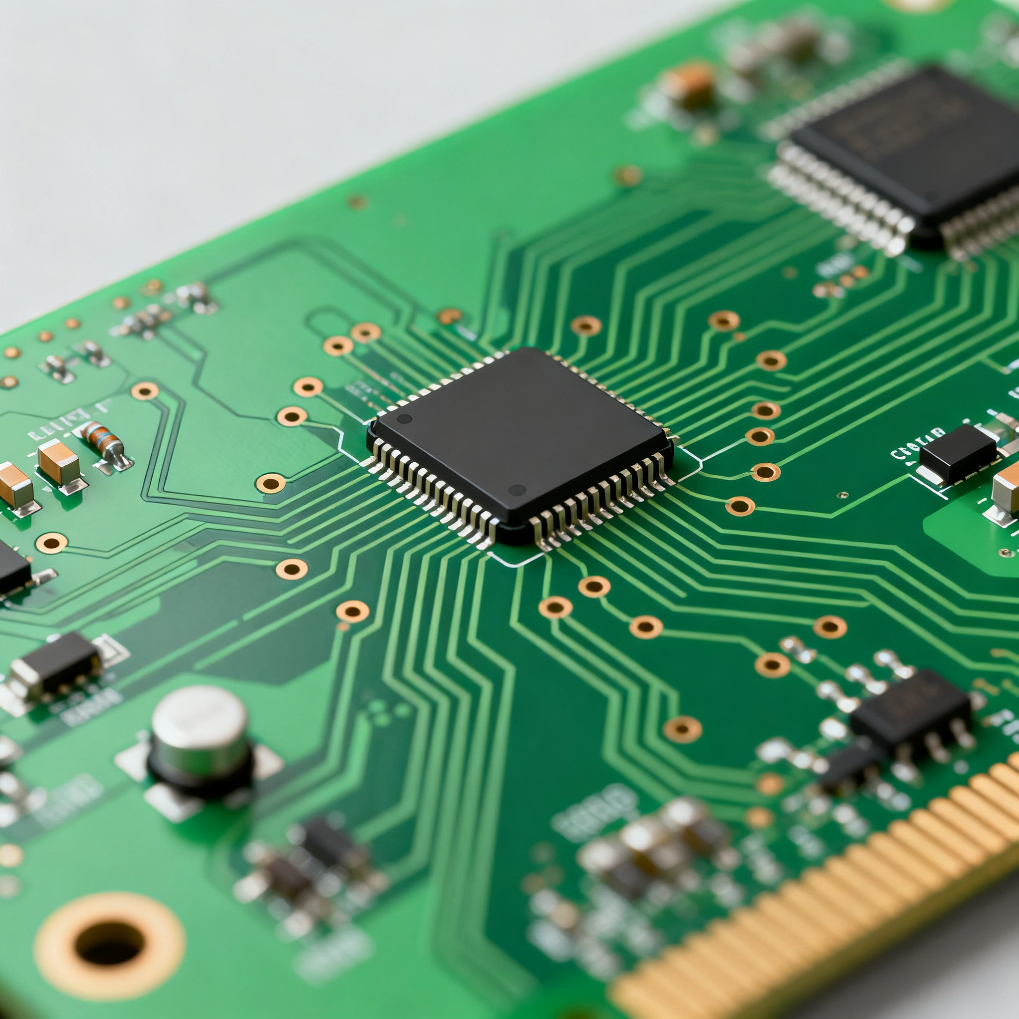
Advanced PCB Design Techniques: Real-World Applications of HDI and Blind/Buried Vias
Advanced PCB Design Techniques: Real-World Applications of HDI and Blind/Buried Vias Introduction In the realm of modern electronics, the demand for compact, high-performance devices is ever-increasin...
Introduction
In the realm of modern electronics, the demand for compact, high-performance devices is ever-increasing. This has led to the adoption of advanced PCB (Printed Circuit Board) design techniques such as High-Density Interconnect (HDI) and the use of blind/buried vias. These techniques enable designers to pack more functionality into smaller spaces, reduce signal loss, and improve overall device performance. Understanding these advanced techniques is crucial for engineers aiming to innovate in fields such as telecommunications, consumer electronics, and automotive systems.
Technical Overview
HDI technology is characterized by the use of microvias, blind vias, and buried vias. Microvias are extremely small vias that connect layers in a PCB, allowing for higher wiring density and more connections in a given area. Blind vias connect an outer layer to an inner layer without going through the entire board, while buried vias connect inner layers only. These technologies reduce the number of layers required and improve signal integrity by minimizing electrical path lengths. The architecture of HDI PCBs often involves sequential lamination, where additional layers are added as needed, allowing for complex multilayer designs.
Detailed Specifications
When selecting components for advanced PCB designs, understanding core specifications is vital. These specifications include CPU speed, memory capacity, available peripherals, power requirements, and the physical package of the components. Such data is crucial for ensuring compatibility, performance, and efficiency in the final product.
| Specification | Details | Comments |
|---|---|---|
| CPU Speed | 1.5 GHz | High-speed processing for complex computations |
| Memory | 4GB DDR4 | Sufficient for multitasking applications |
| Peripherals | USB 3.0, HDMI, Ethernet | Supports high-speed data transfer |
| Power | 5V, 2A | Efficient power consumption for portable devices |
| Package | BGA 256 | Ball Grid Array for compact design |
| Temperature Range | -40°C to 85°C | Suitable for industrial applications |
| Operating Voltage | 3.3V | Standard logic level |
| Storage | 64GB eMMC | Fast access and ample storage space |
| Connectivity | Wi-Fi, Bluetooth | Wireless communication capabilities |
| Dimensions | 50mm x 50mm | Compact form factor |
Key Takeaways from the Specifications
The core specifications table highlights the critical parameters that define the performance and suitability of a component for a given application. For instance, a CPU speed of 1.5 GHz ensures capability for demanding processing tasks, while 4GB DDR4 memory supports efficient multitasking. The inclusion of various peripherals like USB 3.0 and HDMI allows for flexible connectivity options. Power requirements of 5V, 2A are optimal for portable devices, balancing performance and battery life. Understanding these specifications helps engineers select components that meet design goals and operational requirements.
| Electrical Characteristic | Value | Impact |
|---|---|---|
| Supply Voltage | 3.3V | Standard for most digital ICs |
| Max Current | 500mA | Defines power handling capacity |
| Input Voltage Range | 1.8V - 3.3V | Flexibility in power supply design |
| Output High Voltage | 2.9V | Ensures proper logic levels |
| Output Low Voltage | 0.4V | Ensures proper logic levels |
| Propagation Delay | 5ns | Affects signal timing and speed |
| Power Dissipation | 1W | Thermal management considerations |
| Input Capacitance | 5pF | Influences signal integrity |
| Operating Frequency | 100MHz | Determines speed of operation |
| Leakage Current | 10µA | Impacts standby power consumption |
Practical Implications
The electrical characteristics table provides insight into the operational limits and performance of components. A supply voltage of 3.3V is typical for digital circuits, ensuring compatibility with other ICs. The max current of 500mA dictates the power delivery requirements, while propagation delay of 5ns suggests fast signal processing. Power dissipation of 1W requires effective thermal management to avoid overheating. Understanding these values is crucial for optimizing circuit performance and ensuring reliability under varied conditions.
| Application | Configuration | Benefits |
|---|---|---|
| Smartphones | HDI with microvias | Increased functionality in compact form |
| Automotive Electronics | Blind/buried vias | Improved reliability and signal integrity |
| Wearable Devices | Flexible PCB with HDI | Enhanced durability and flexibility |
| Telecommunication Equipment | Multilayer HDI | High-speed data transmission |
| Medical Devices | Miniaturized HDI | Precision and compactness |
| Industrial Automation | Rugged HDI | Robustness in harsh environments |
Application Guidelines
The application comparison table illustrates the diverse use cases and configurations of HDI and blind/buried vias. For smartphones, HDI with microvias allows for more components in a smaller space, enhancing functionality. Automotive electronics benefit from blind/buried vias, which improve reliability and signal integrity critical for safety systems. Wearable devices leverage flexible PCBs with HDI for enhanced durability, while telecommunication equipment relies on multilayer HDI for high-speed data handling. Understanding these configurations helps engineers tailor designs to specific application needs, optimizing performance and reliability.
Design Considerations
Advanced PCB design requires careful consideration of several factors to ensure optimal performance and manufacturability. The choice of via type—whether it be microvias, blind, or buried vias—depends on the specific application requirements such as layer count and signal paths. Signal integrity is a critical concern, necessitating careful impedance control and minimizing crosstalk through proper trace routing and spacing. Thermal management is also vital, especially in high-power applications, requiring the use of thermal vias and heat sinks to dissipate heat effectively. Additionally, material selection for the PCB substrate impacts dielectric properties and mechanical robustness, influencing the overall reliability of the design. By adhering to industry standards like IPC-2221, designers can ensure compliance and quality in their PCB layouts.
Step-by-Step Implementation
- Define the project requirements, including size, power, and functionality.
- Select the appropriate PCB substrate material based on thermal and electrical properties.
- Design the schematic, focusing on component placement and signal flow.
- Choose the via types and layer stack-up to optimize space and signal integrity.
- Route traces with attention to impedance control and minimizing signal interference.
- Perform thermal analysis and incorporate heat dissipation features.
- Verify design compliance with IPC standards and perform DFM checks.
- Prototype and test the PCB to validate performance against design specifications.
Common Issues & Solutions
- Issue: Signal interference due to improper trace routing. Solution: Use differential pairs and maintain consistent trace width and spacing.
- Issue: Thermal hotspots causing component failure. Solution: Integrate thermal vias and heat sinks to improve heat dissipation.
- Issue: Insufficient power delivery to components. Solution: Optimize power plane design and use low-impedance paths.
- Issue: Manufacturing defects due to complex via structures. Solution: Collaborate with manufacturers early in the design process to ensure feasibility.
- Issue: High crosstalk in dense signal areas. Solution: Use ground planes and careful trace shielding to minimize interference.
- Issue: Inconsistent board performance in different environments. Solution: Test the PCB across a range of temperatures and conditions to ensure reliability.
Applications & Use Cases
Advanced PCB designs using HDI and blind/buried vias are prevalent across multiple industries. In consumer electronics, they enable the miniaturization of devices like smartphones and tablets, offering more features without increasing size. In automotive systems, these technologies provide the reliability and performance needed for advanced safety and infotainment systems. Telecommunication infrastructure benefits from high-speed, high-density PCBs that handle large volumes of data. Medical devices leverage these designs for precision and compactness, critical in portable diagnostic tools. Each application requires careful consideration of design trade-offs to meet specific performance and reliability criteria.
Selection & Sourcing Guide
When selecting components and materials for advanced PCB designs, engineers should consider factors such as performance specifications, compatibility, and cost. Reliable sourcing is crucial for maintaining quality and consistency. IC Online offers a comprehensive selection of components tailored for high-performance PCB applications, providing detailed datasheets and technical support to aid in the selection process.
FAQ
- Q: What are the benefits of using HDI technology in PCB design? A: HDI technology allows for higher component density, improved signal integrity, and reduced board size.
- Q: How do blind and buried vias improve PCB performance? A: They reduce the number of layers required and shorten electrical paths, enhancing signal speed and integrity.
- Q: What materials are best for high-frequency PCB applications? A: Materials with low dielectric loss, such as PTFE, are ideal for high-frequency applications.
- Q: How do I ensure my PCB design complies with industry standards? A: Adhere to IPC standards and perform thorough design for manufacturability (DFM) checks.
- Q: What are common challenges in HDI PCB manufacturing? A: Challenges include precise microvia drilling and maintaining signal integrity in dense layouts.
- Q: How can I minimize thermal issues in my PCB design? A: Use thermal vias, heat sinks, and proper layout techniques to manage heat effectively.
- Q: What role do vias play in multilayer PCB design? A: Vias connect different layers, enabling complex routing and efficient use of space.
- Q: How important is impedance control in advanced PCB designs? A: Critical for maintaining signal integrity, especially in high-speed and RF applications.
- Q: What are the cost implications of using HDI and blind/buried vias? A: While they increase manufacturing complexity and cost, they provide significant performance benefits.
- Q: Can HDI technology be used in flexible PCBs? A: Yes, HDI can be integrated into flexible PCBs, enhancing their functionality and durability.
Conclusion
Advanced PCB design techniques such as HDI and blind/buried vias are essential for creating high-performance, compact electronic devices. By understanding the core specifications, electrical characteristics, and application guidelines, engineers can design PCBs that meet the demands of modern technology. As these technologies continue to evolve, staying informed about the latest standards and best practices is crucial for success in the field of electronics engineering.